M4A5-384/128-5SAC –ü—Ä–ĺ—Ā–ľ–ĺ—ā—Ä —ā–Ķ—Ö–Ĺ–ł—á–Ķ—Ā–ļ–ĺ–≥–ĺ –ĺ–Ņ–ł—Ā–į–Ĺ–ł—Ź (PDF) - Lattice Semiconductor
–Ě–ĺ–ľ–Ķ—Ä –≤ –ļ–į—ā–į–Ľ–ĺ–≥–Ķ
–ö–ĺ–ľ–Ņ–ĺ–Ĺ–Ķ–Ĺ—ā—č –ě–Ņ–ł—Ā–į–Ĺ–ł–Ķ
–Ņ—Ä–ĺ–ł–∑–≤–ĺ–ī–ł—ā–Ķ–Ľ—Ć
M4A5-384/128-5SAC
Lattice Semiconductor

M4A5-384/128-5SAC Datasheet PDF : 63 Pages
| |||
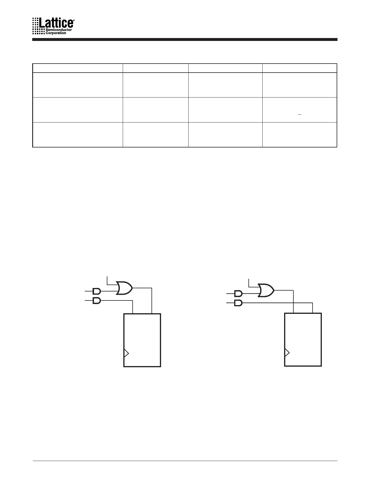
Table 8. Register/Latch Operation
ConÔ¨Āguration
Input(s)
CLK/LE 1
Q+
D-type Register
D=X
0,1, ‚Üď (‚ÜĎ)
Q
D=0
‚ÜĎ (‚Üď)
0
D=1
‚ÜĎ (‚Üď)
1
T-type Register
T=X
0, 1, ‚Üď (‚ÜĎ)
Q
T=0
‚ÜĎ (‚Üď)
Q
T=1
‚ÜĎ (‚Üď)
Q
D=X
1 (0)
Q
D-type Latch
D=0
0 (1)
0
D=1
0 (1)
1
Note:
1. Polarity of CLK/LE can be programmed
Although the macrocell shows only one input to the register, the XOR gate in the logic allocator allows the
D-, T-type register to emulate J-K, and S-R behavior. In this case, the available product terms are divided
between J and K (or S and R). When configured as J-K, S-R, or T-type, the extra product term must be used
on the XOR gate input for flip-flop emulation. In any register type, the polarity of the inputs can be
programmed.
The clock input to the flip-flop can select any of the four PAL block clocks in synchronous mode, with the
additional choice of either polarity of an individual product term clock in the asynchronous mode.
The initialization circuit depends on the mode. In synchronous mode (Figure 7), asynchronous reset and
preset are provided, each driven by a product term common to the entire PAL block.
Power-Up
Reset
PAL-Block
Initialization
Product Terms
AP AR
D/T/L Q
Power-Up
Preset
PAL-Block
Initialization
Product Terms
AP AR
D/L
Q
a. Power-up reset
b. Power-up preset
17466G-012
Figure 7. Synchronous Mode Initialization ConÔ¨Āgurations
17466G-013
12
ispMACH 4A Family
Share Link: