PI74FCT162652T Просмотр технического описания (PDF) - Pericom Semiconductor
Номер в каталоге
Компоненты Описание
производитель
PI74FCT162652T Datasheet PDF : 6 Pages
| |||
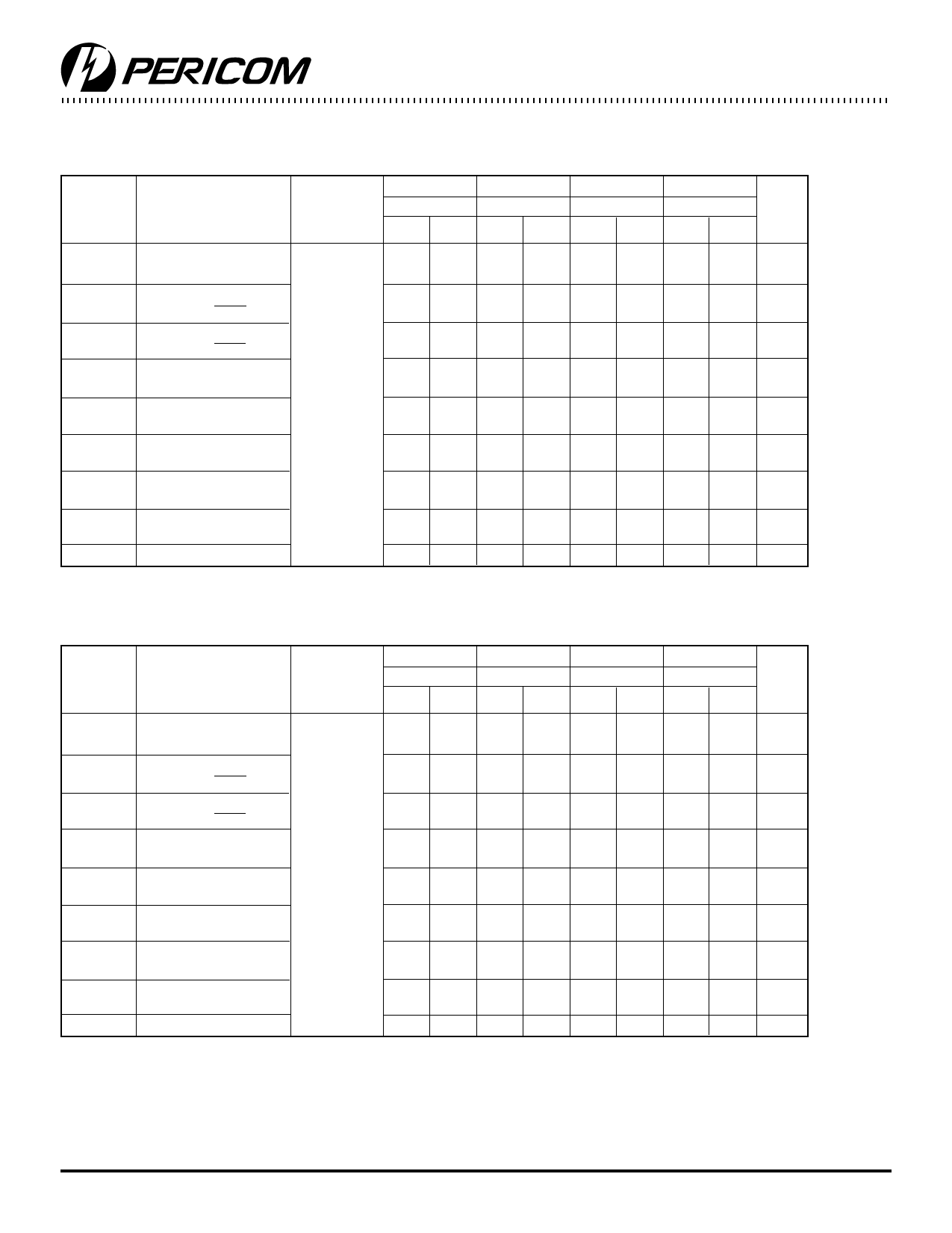
PI74FCT16652/162652T
12345678901234567890123456789012123456789012345678901234567890121234567890123456789011623-4B56I7T890R12E12G345I6S78T90E12R34E56D789T01R234A56N78S90C12E12I3V456E78R90S12
PI74FCT16652 Switching Characteristics over Operating Range
Parameters Description
16652T
16652AT
16652CT
16652DT
Com.
Com.
Com.
Com.
Conditions(1) Min Max Min Max Min Max Min Max Unit
tPLH
Propagation Delay
CL = 50 pF 2.0 9.0 2.0 6.3 1.5 5.4 1.5 4.4 ns
tPHL
Bus to Bus
RL = 500Ω
tPZH
Output Enable Time
2.0 14.0 2.0 9.8 1.5 7.8 1.5 5.0 ns
tPZL
XOEAB or X OEBA to Bus
tPHZ
Output Disable Time(3)
2.0 9.0 2.0 6.3 1.5 6.3 1.5 4.3 ns
tPLZ
XOEAB or X OEBA to Bus
tPLH
Propagation Delay
2.0 9.0 2.0 6.3 1.5 5.7 1.5 4.4 ns
tPHL
Clock to Bus
tPLH
Propagation Delay
2.0 11.0 2.0 7.7 1.5 6.2 1.5 5.0 ns
tPHL
xSBA or xSAB to Bus
tSU
Setup Time HIGH or
4.0 — 2.0 — 2.0 — 2.0 — ns
LOW, BUS to Clock
tH
Hold Time HIGH or
2.0 — 1.5 — 1.5 — 1.0 — ns
LOW, Bus to Clock
tW
Clock Pulse Width
6.0 — 5.0 — 5.0 — 3.0 — ns
HIGH or LOW(3)
tSK(o)
Output Skew(4)
— 0.5 — 0.5 — 0.5 — 0.5 ns
PI74FCT162652 Switching Characteristics over Operating Range
Parameters Description
Conditions(1)
162652T
162652AT
162652CT
162652DT
Com.
Com.
Com.
Com.
Min Max Min Max Min Max Min Max Unit
tPLH
Propagation Delay
CL = 50 pF
2.0 9.0 2.0 6.3 1.5 5.4 1.5 4.4 ns
tPHL
Bus to Bus
RL = 500Ω
tPZH
Output Enable Time
2.0 14.0 2.0 9.8 1.5 7.8 1.5 5.0 ns
tPZL
XOEAB or X OEBA to Bus
tPHZ
Output Disable Time(3)
2.0 9.0 2.0 6.3 1.5 6.3 1.5 4.3 ns
tPLZ
XOEAB or X OEBA to Bus
tPLH
Propagation Delay
2.0 9.0 2.0 6.3 1.5 5.7 1.5 4.4 ns
tPHL
Clock to Bus
tPLH
Propagation Delay
2.0 11.0 2.0 7.7 1.5 6.2 1.5 5.0 ns
tPHL
xSBA or xSAB to Bus
tSU
Setup Time HIGH or
4.0 — 2.0 — 2.0 — 2.0 — ns
LOW, BUS to Clock
tH
Hold Time HIGH or
2.0 — 1.5 — 1.5 — 1.0 — ns
LOW, Bus to Clock
tW
Clock Pulse Width
6.0 — 5.0 — 5.0 — 3.0 — ns
HIGH or LOW(3)
tSK(o)
Output Skew(4)
— 0.5 — 0.5 — 0.5 — 0.5 ns
Notes:
1. See test circuit and wave forms.
2. Minimum limits are guaranteed but not tested on Propagation Delays.
3. This limit is guaranteed but not production tested.
4. Skew between any two outputs, of the same package, switching in the same direction. This parameter is guaranteed by design.
6
PS2079A 01/15/95
Share Link: 