LC74761 Просмотр технического описания (PDF) - SANYO -> Panasonic
Номер в каталоге
Компоненты Описание
производитель
LC74761 Datasheet PDF : 21 Pages
| |||
LC74761, LC74761M
Display Control Commands
Display control commands are input in an 8-bit serial format. Commands consist of a command identification code in the
first byte and data in the second and following bytes. The following commands are supported.
1 COMMAND0: Display memory (VRAM) write address setting command
2 COMMAND1: Display character data write command
3 COMMAND2: Vertical display start position and character size (lines 1 and 2) setting command
4 COMMAND3: Horizontal display start position and character size (lines 9 and 11) setting command
5 COMMAND4: Display control setting command 1
6 COMMAND5: Display control setting command 2
7 COMMAND6: Display control setting command 3
8 COMMAND7: Display control setting command 4
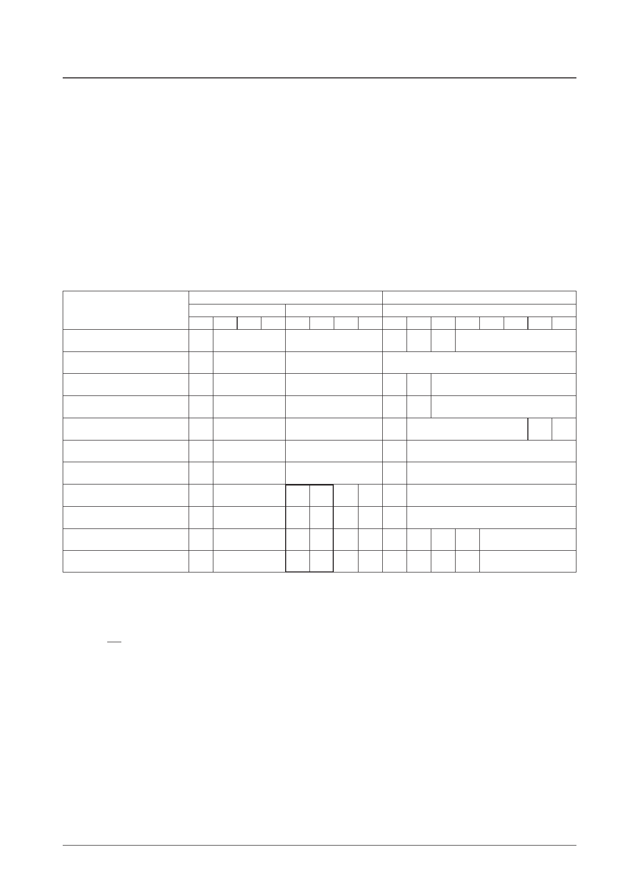
Display Control Command Table
Command
COMMAND0
Write address
COMMAND1
Character write
COMMAND2
Vertical display start position
COMMAND3
Horizontal display start position
COMMAND4
Display control 1
COMMAND5
Display control 2
COMMAND6
Display control 3
COMMAND70
Display control 4
COMMAND71
Display control 5
COMMAND72
Display control 6
COMMAND73
Display control 7
First byte
Second byte
Command identification code
Data
Data
7
6
5
4
3
2
1
0
7
6
5
4
3
2
1
0
1
0
0
0 V3 V2 V1 V0 0
0
0 H4 H3 H2 H1 H0
1
0
0
1
0
0 at2 at1 c7 c6 c5 c4 c3 c2 c1 c0
1
0
1
0 SZ SZ SZ SZ 0
0 VP VP VP VP VP VP
21 20 11 10
5
4
3
2
1
0
1
0
1
1 SZ SZ SZ SZ 0
0 HP HP HP HP HP HP
B1 B0 91 90
5
4
3
2
1
0
1
1
0
0 RST RAM OSC RND 0 I/N BLK BLK BK ATS 0 DSP
1
0
1
1
1
0
1 PH PH PH I/E 0 TST CHAL BLK RSL RSL CVM XTS
2
1
0
1
0
1
1
1
0 MOD MOD MOD MOD 0 HFI M30S SMS IOS BCL BCL CB
3
2
1
0
1
0
1
1
1
1
0
0
0 LINS 0 VCOS LIN LIN LIN LIN LIN LIN
1
5
4
3
2
1
0
1
1
1
1
0
1
0 LINS 0 EG PS PS VMN SVIS VNS VSS
2
2
1
1
1
1
1
1
0
0 LINS 0
0
0
0 MOD MOD MOD MOD
3
2
1
0
1
1
1
1
1
1
0 LINS 0
0
0
0 VCOS SOUT VOUT HOUT
2
Once the command identification code in the first bite is written, it is stored internally until the first byte of the following
command is written. However, when the display character data write command (COMMAND1) is written, the system
becomes locked in display character data write mode, and the first byte cannot be overwritten.
When the CS pin is set high the command state is set to COMMAND0, i.e., display memory write address setting mode.
No. 4846-7/21
Share Link: 