M25P16-VMN3 Просмотр технического описания (PDF) - Micron Technology
Номер в каталоге
Компоненты Описание
производитель
M25P16-VMN3 Datasheet PDF : 62 Pages
| |||
Signal Descriptions
Micron M25P16 Serial Flash Embedded Memory
Signal Descriptions
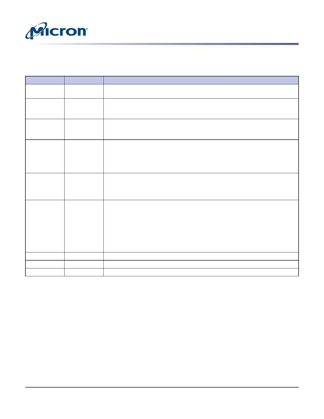
Table 2: Signal Descriptions
Signal
DQ1
DQ0
C
S#
HOLD#
W#/VPP
VCC
VSS
DNU
Type
Output
Input
Input
Input
Input
Input
Power
Ground
–
Description
Serial data: The DQ1 output signal is used to transfer data serially out of the device.
Data is shifted out on the falling edge of the serial clock (C).
Serial data: The DQ0 input signal is used to transfer data serially into the device. It
receives commands, addresses, and the data to be programmed. Values are latched on
the rising edge of the serial clock (C).
Clock: The C input signal provides the timing of the serial interface. Commands, ad-
dresses, or data present at serial data input (DQ0) is latched on the rising edge of the
serial clock (C). Data on DQ1 changes after the falling edge of C.
Chip select: When the S# input signal is HIGH, the device is deselected and DQ1 is at
high impedance. Unless an internal PROGRAM, ERASE, or WRITE STATUS REGISTER cy-
cle is in progress, the device will be in the standby power mode (not the deep power-
down mode). Driving S# LOW enables the device, placing it in the active power mode.
After power-up, a falling edge on S# is required prior to the start of any command.
Hold: The HOLD# signal is used to pause any serial communications with the device
without deselecting the device. During the hold condition, DQ1 is High-Z. DQ0 and C
are "Don’t Care." To start the hold condition, the device must be selected, with S#
driven LOW.
Write protect: The W#/VPP signal is both a control input and a power supply pin. The
two functions are selected by the voltage range applied to the pin. If the W#/VPP input
is kept in a low voltage range (0 V to VCC) the pin is seen as a control input. The W#
input signal is used to freeze the size of the area of memory that is protected against
program or erase commands as specified by the values in BP2, BP1, and BP0 bits of the
Status Register. VPP acts as an additional power supply if it is in the range of VPPH, as
defined in the AC Measurement Conditions table. Avoid applying VPPH to the W#/VPP
pin during a BULK ERASE operation.
Device core power supply: Source voltage.
Ground: Reference for the VCC supply voltage.
Do not use.
PDF: 09005aef8456656c
m25p16.pdf - Rev. J 1/18 EN
9
Micron Technology, Inc. reserves the right to change products or specifications without notice.
© 2011 Micron Technology, Inc. All rights reserved.
Share Link: 