EN5335QI Просмотр технического описания (PDF) - Altera Corporation
Номер в каталоге
Компоненты Описание
производитель
EN5335QI Datasheet PDF : 15 Pages
| |||
EN5335QI
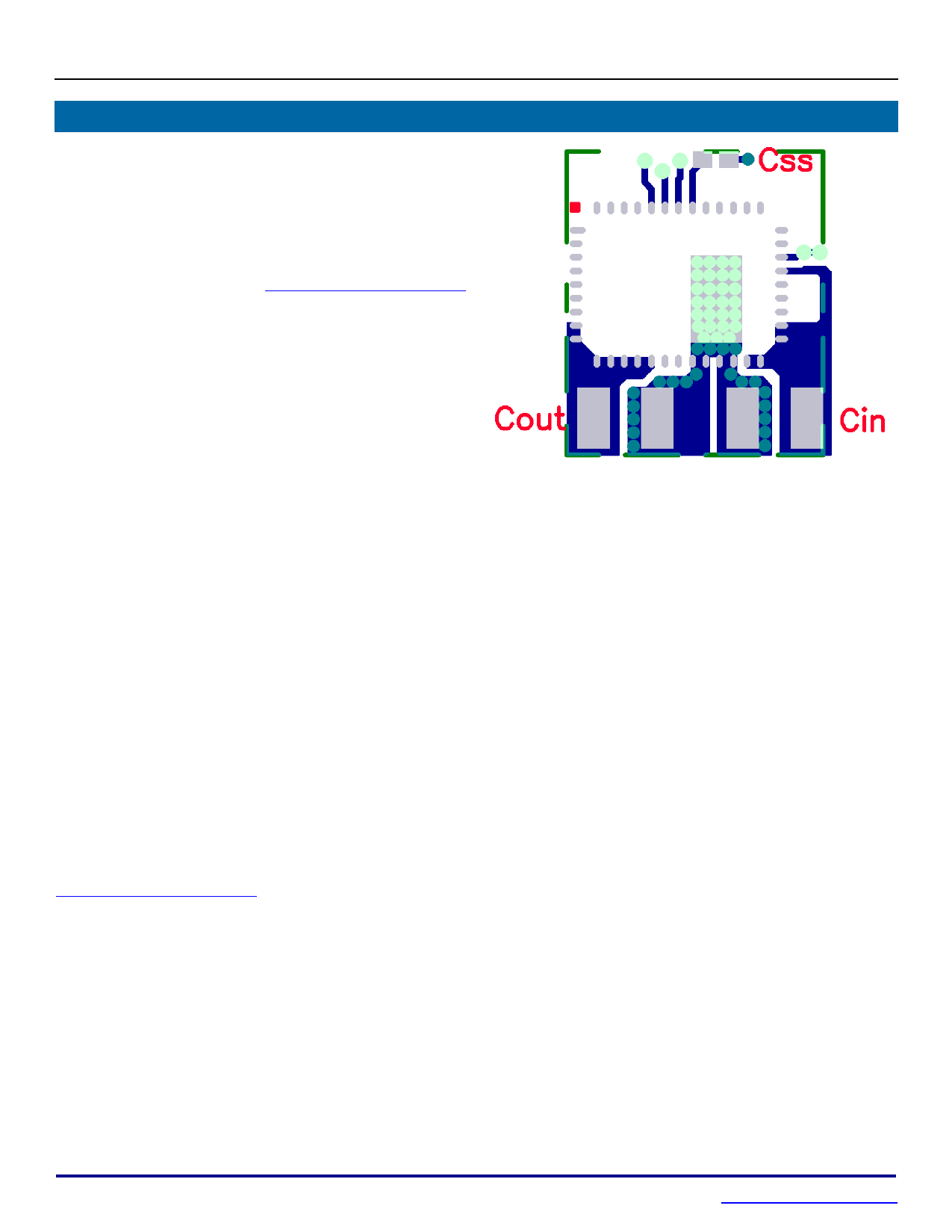
Layout Recommendation
Figure 4 shows critical components and layer 1
traces of a recommended minimum footprint
EN5335QI layout. Alternate ENABLE
configurations and other small signal pins need
to be connected and routed according to specific
customer application. Please see the Gerber files
on the Altera website www.altera.com/enpirion
for exact dimensions and other layers. Please
refer to Figure 4 while reading the layout
recommendations in this section.
Recommendation 1: Input and output filter
capacitors should be placed on the same side of
the PCB, and as close to the EN5335QI package
as possible. They should be connected to the
device with very short and wide traces. Do not
use thermal reliefs or spokes when connecting
the capacitor pads to the respective nodes. The
+V and GND traces between the capacitors and
the EN5335QI should be as close to each other
as possible so that the gap between the two
nodes is minimized, even under the capacitors.
Recommendation 2: Two PGND pins are
dedicated to the input circuit, and two to the
output circuit. The slit in Figure 4 separating the
input and output GND circuits helps minimize
noise coupling between the converter input and
output switching loops.
Recommendation 3: The system ground plane
should be the first layer immediately below the
surface layer. This ground plane should be
continuous and un-interrupted below the
converter and the input/output capacitors. Please
see the Gerber files on the Altera website
www.altera.com/enpirion.
Recommendation 4: The large thermal pad
underneath the component must be connected to
the system ground plane through as many vias
as possible.
Figure 4: Top PCB Layer Critical Components
and Copper for Minimum Footprint
The drill diameter of the vias should be 0.33mm,
and the vias must have at least 1 oz. copper
plating on the inside wall, making the finished
hole size around 0.20-0.26mm. Do not use
thermal reliefs or spokes to connect the vias to
the ground plane. This connection provides the
path for heat dissipation from the converter.
Please see Figures: 7, 8, and 9.
Recommendation 5: Multiple small vias (the
same size as the thermal vias discussed in
recommendation 4 should be used to connect
ground terminal of the input capacitor and output
capacitors to the system ground plane. It is
preferred to put these vias under the capacitors
along the edge of the GND copper closest to the
+V copper. Please see Figure 4. These vias
connect the input/output filter capacitors to the
GND plane, and help reduce parasitic
inductances in the input and output current loops.
If the vias cannot be placed under CIN and COUT,
then put them just outside the capacitors along
the GND slit separating the two components. Do
not use thermal reliefs or spokes to connect
these vias to the ground plane.
Recommendation 6: AVIN is the power supply
for the internal small-signal control circuits. It
should be connected to the input voltage at a
quiet point. In Figure 4 this connection is made at
00846
11
October 11, 2013
www.altera.com/enpirion
Rev J
Share Link: 