LH168A Просмотр технического описания (PDF) - Sharp Electronics
Номер в каталоге
Компоненты Описание
производитель
LH168A Datasheet PDF : 14 Pages
| |||
LH168A
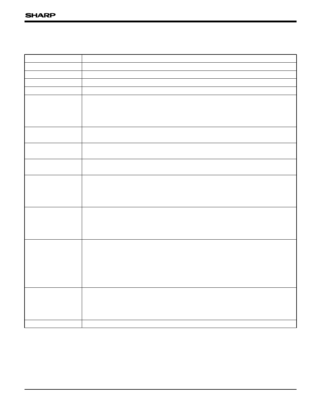
FUNCTIONAL DESCRIPTION
Pin Functions
SYMBOL
VCC
VLS
GNDL
GNDA
SPIO
SPOI
LBR
LS
CK
V1-V10
XA0-XA5, YA0-YA5
ZA0-ZA5, XB0-XB5
YB0-YB5, ZB0-ZB5
XO1-XO128,
YO1-YO128,
ZO1-ZO128
POL1
POL2
TESTB
FUNCTIONS
Used as power supply pin for digital circuit, connected to +2.7 to +3.6 V.
Used as power supply pin for analog circuit, connected to +3.0 to +5.5 V.
Used as ground pin for logic circuit, connected to 0 V.
Used as ground pin for LCD drive circuit, connected to 0 V.
Used as input pins of start pulse and also used as output pins for cascade connection.
When "H" is input into start pulse input pin, data sampling is started. On completion of
sampling, "H" pulse is output to output pin for cascade connection. Pin functions are
selected by LBR. For selecting, refer to "Functional Operations".
Used as input pin for selecting the shift register direction. For selecting, refer to
"Functional Operations".
Used as input pin for parallel transfer from sampling memory to hold memory. Data is
transferred at the rising edge and output from LCD drive output pin.
Used as shift clock input pin. Data is latched into sampling memory from data input pin at
the rising edge.
Used as reference voltage input pins. Hold the reference voltage fixed during the period of
LCD drive output. For relation between input data and output voltage values, refer to
"Output Voltage Value". For internal gamma correction, refer to "Gamma Correction
Value".
Used as data input pins of R, G, and B colors. 6-bit x 2-pixel data are input from data pins
at the rising edge of CK. For relation between input data and output voltage values, refer
to "Functional Operations" and "Output Voltage Value". Select the data to be entered
into X, Y, and Z according to picture element arrays of the panel.
Used as LCD drive output pins which output the voltage corresponding to the input of data
input pins (XA0 to XA5, XB0 to XB5, YA0 to YA5, YB0 to YB5, ZA0 to ZA5, ZB0 to ZB5).
Data of XO1 to XO128 correspond to XA0 to XA5 and XB0 to XB5. Data of YO1 to YO128
correspond to YA0 to YA5 and YB0 to YB5, and data of ZO1 to ZO128 correspond to ZA0 to
ZA5 and ZB0 to ZB5. For relation between input data and output voltage values, refer to
"Functional Operations" and "Output Voltage Value".
Used as input pins for input data polarity exchange. When "L" is entered, display data
becomes normal mode. When "H" is entered, input data becomes polarity exchange mode
(POL1 = A system, POL2 = B system). For relation between input data and output voltage
values, refer to "Output Voltage Value". Must be connected to 0 V or opened.
Used as pin for IC testing. Must be connected to VCC or opened.
6
Share Link: 