MC100EP11(2003) Просмотр технического описания (PDF) - ON Semiconductor
Номер в каталоге
Компоненты Описание
производитель
MC100EP11 Datasheet PDF : 8 Pages
| |||
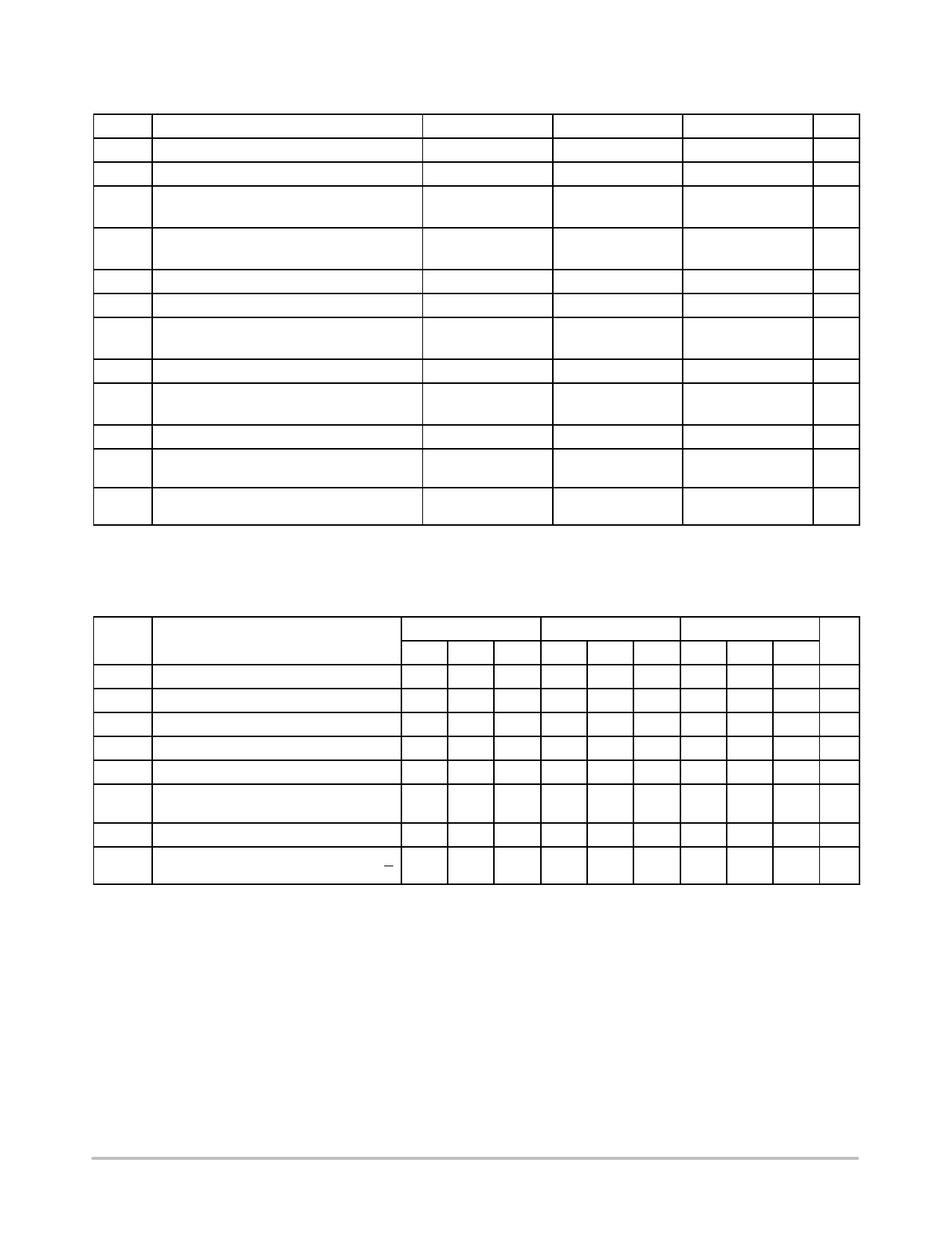
MC10EP11, MC100EP11
10EP DC CHARACTERISTICS, PECL VCC = 3.3 V, VEE = 0 V (Note 3)
−40°C
25°C
85°C
Symbol
Characteristic
Min Typ Max Min Typ Max Min Typ Max Unit
IEE
Negative Power Supply Current
20
29
37
20
30
39
22
31
40 mA
VOH
Output HIGH Voltage (Note 4)
2165 2290 2415 2230 2355 2480 2290 2415 2540 mV
VOL
Output LOW Voltage (Note 4)
1365 1490 1615 1430 1555 1680 1490 1615 1740 mV
VIH
Input HIGH Voltage (Single−Ended)
2090
2415 2155
2480 2215
2540 mV
VIL
Input LOW Voltage (Single−Ended)
1365
1690 1430
1755 1490
1815 mV
VIHCMR Input HIGH Voltage Common Mode
2.0
Range (Differential Configuration) (Note 5)
3.3 2.0
3.3 2.0
3.3 V
IIH
Input HIGH Current
IIL
Input LOW Current
D 0.5
D −150
150
0.5
−150
150
0.5
−150
150 mA
mA
NOTE: EP circuits are designed to meet the DC specifications shown in the above table after thermal equilibrium has been established.
The circuit is in a test socket or mounted on a printed circuit board and transverse airflow greater than 500 lfpm is maintained.
3. Input and output parameters vary 1:1 with VCC. VEE can vary +0.3 V to −2.2 V.
4. All loading with 50 W to VCC − 2.0 V.
5. VIHCMR min varies 1:1 with VEE, VIHCMR max varies 1:1 with VCC. The VIHCMR range is referenced to the most positive side of the differen-
tial input signal.
10EP DC CHARACTERISTICS, PECL VCC = 5.0 V, VEE = 0 V (Note 6)
−40°C
25°C
85°C
Symbol
Characteristic
Min Typ Max Min Typ Max Min Typ Max Unit
IEE
Negative Power Supply Current
20
29
37
20
30
39
22
31
40 mA
VOH
Output HIGH Voltage (Note 7)
3865 3990 4115 3930 4055 4180 3990 4115 4240 mV
VOL
Output LOW Voltage (Note 7)
3065 3190 3315 3130 3255 3380 3190 3315 3440 mV
VIH
Input HIGH Voltage (Single−Ended)
3790
4115 3855
4180 3915
4240 mV
VIL
Input LOW Voltage (Single−Ended)
3065
3390 3130
3455 3190
3515 mV
VIHCMR Input HIGH Voltage Common Mode
2.0
Range (Differential Configuration) (Note 8)
5.0 2.0
5.0 2.0
5.0 V
IIH
Input HIGH Current
IIL
Input LOW Current
D 0.5
D −150
150
0.5
−150
150
0.5
−150
150 mA
mA
NOTE: EP circuits are designed to meet the DC specifications shown in the above table after thermal equilibrium has been established.
The circuit is in a test socket or mounted on a printed circuit board and transverse airflow greater than 500 lfpm is maintained.
6. Input and output parameters vary 1:1 with VCC. VEE can vary +2.0 V to −0.5 V.
7. All loading with 50 W to VCC − 2.0 V.
8. VIHCMR min varies 1:1 with VEE, VIHCMR max varies 1:1 with VCC. The VIHCMR range is referenced to the most positive side of the differen-
tial input signal.
10EP DC CHARACTERISTICS, NECL VCC = 0 V; VEE = −5.5 V to −3.0 V (Note 9)
−40°C
25°C
85°C
Symbol
IEE
VOH
VOL
VIH
VIL
VIHCMR
Characteristic
Negative Power Supply Current
Output HIGH Voltage (Note 10)
Output LOW Voltage (Note 10)
Input HIGH Voltage (Single−Ended)
Input LOW Voltage (Single−Ended)
Input HIGH Voltage Common Mode
Range (Differential Configuration)
(Note 11)
Min Typ Max Min Typ Max Min Typ Max Unit
20
29
37
20
30
39
22
31
40 mA
−1135 −1010 −885 −1070 −945 −820 −1010 −885 −760 mV
−1935 −1810 −1685 −1870 −1745 −1620 −1810 −1685 −1560 mV
−1210
−885 −1145
−820 −1085
−760 mV
−1935
−1610 −1870
−1545 −1810
−1485 mV
VEE+2.0
0.0
VEE+2.0
0.0
VEE+2.0
0.0 V
IIH
Input HIGH Current
IIL
Input LOW Current
D 0.5
D −150
150
0.5
−150
150
0.5
−150
150 mA
mA
NOTE: EP circuits are designed to meet the DC specifications shown in the above table after thermal equilibrium has been established.
The circuit is in a test socket or mounted on a printed circuit board and transverse airflow greater than 500 lfpm is maintained.
9. Input and output parameters vary 1:1 with VCC.
10. All loading with 50 W to VCC − 2.0 V.
11. VIHCMR min varies 1:1 with VEE, VIHCMR max varies 1:1 with VCC. The VIHCMR range is referenced to the most positive side of the differen-
tial input signal.
http://onsemi.com
3
Share Link: 