74LVC245AD(2009) Просмотр технического описания (PDF) - NXP Semiconductors.
Номер в каталоге
Компоненты Описание
производитель
74LVC245AD Datasheet PDF : 17 Pages
| |||
NXP Semiconductors
74LVC245A; 74LVCH245A
Octal bus transceiver; 3-state
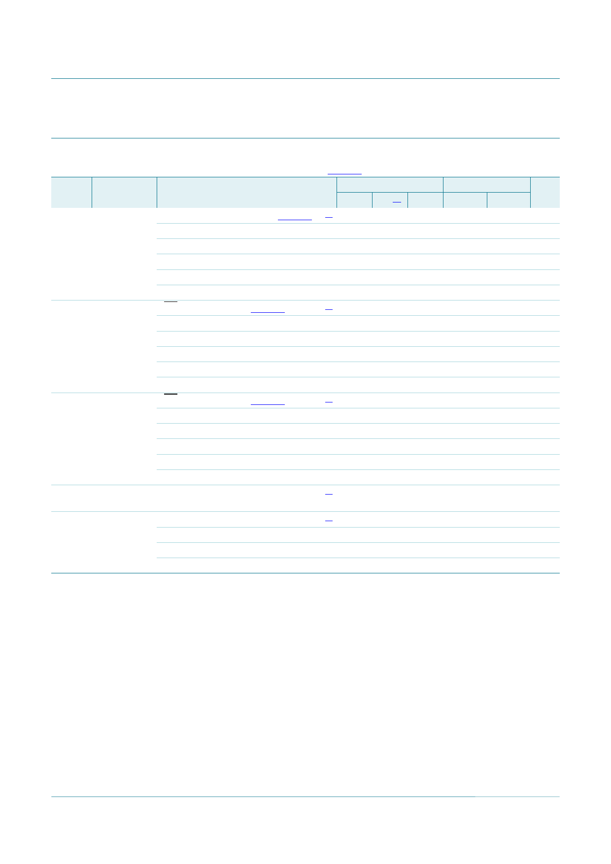
Table 7. Dynamic characteristics …continued
Voltages are referenced to GND (ground = 0 V). For test circuit see Figure 7.
Symbol Parameter Conditions
−40 °C to +85 °C
Min Typ[2] Max
CPD
power
per buffer; VI = GND to VCC; VCC = 3.3 V [5] -
15
-
dissipation
capacitance
−40 °C to +125 °C Unit
Min
Max
-
- pF
[1] tpd is the same as tPLH and tPHL.
ten is the same as tPZL and tPZH.
tdis is the same as tPLZ and tPHZ.
[2] Typical values are measured at Tamb = 25 °C.
[3] Typical values are measured at Tamb = 25 °C and VCC = 3.3 V.
[4] Skew between any two outputs of the same package switching in the same direction. This parameter is guaranteed by design.
[5] CPD is used to determine the dynamic power dissipation (PD in µW).
PD = CPD × VCC2 × fi × N + Σ(CL × VCC2 × fo) where:
fi = input frequency in MHz; fo = output frequency in MHz
CL = output load capacitance in pF
VCC = supply voltage in Volts
N = number of inputs switching
Σ(CL × VCC2 × fo) = sum of the outputs.
11. AC waveforms
VI
An, Bn input
GND
VOH
tPLH
Bn, An output
VOL
VM
VM
VM
tPHL
VM
mna176
Fig 5.
See Table 8 for measurement points
VOL and VOH are typical output voltage levels that occur with the output load.
Input (An, Bn) to output (Bn, An) propagation delays and output transition times
74LVC_LVCH245A_5
Product data sheet
Rev. 05 — 25 August 2009
© NXP B.V. 2009. All rights reserved.
7 of 17
Share Link: 