2N5064 Просмотр технического описания (PDF) - Digitron Semiconductors
Номер в каталоге
Компоненты Описание
производитель
2N5064 Datasheet PDF : 4 Pages
| |||
DIGITRON SEMICONDUCTORS
2N5060-2N5064
SENSITIVE GATE SILICON CONTROLLED RECTIFIERS
Available Non-RoHS (standard) or RoHS compliant (add PBF suffix).
Available as “HR” (high reliability) screened per MIL-PRF-19500, JANTX level. Add “HR” suffix to base part number.
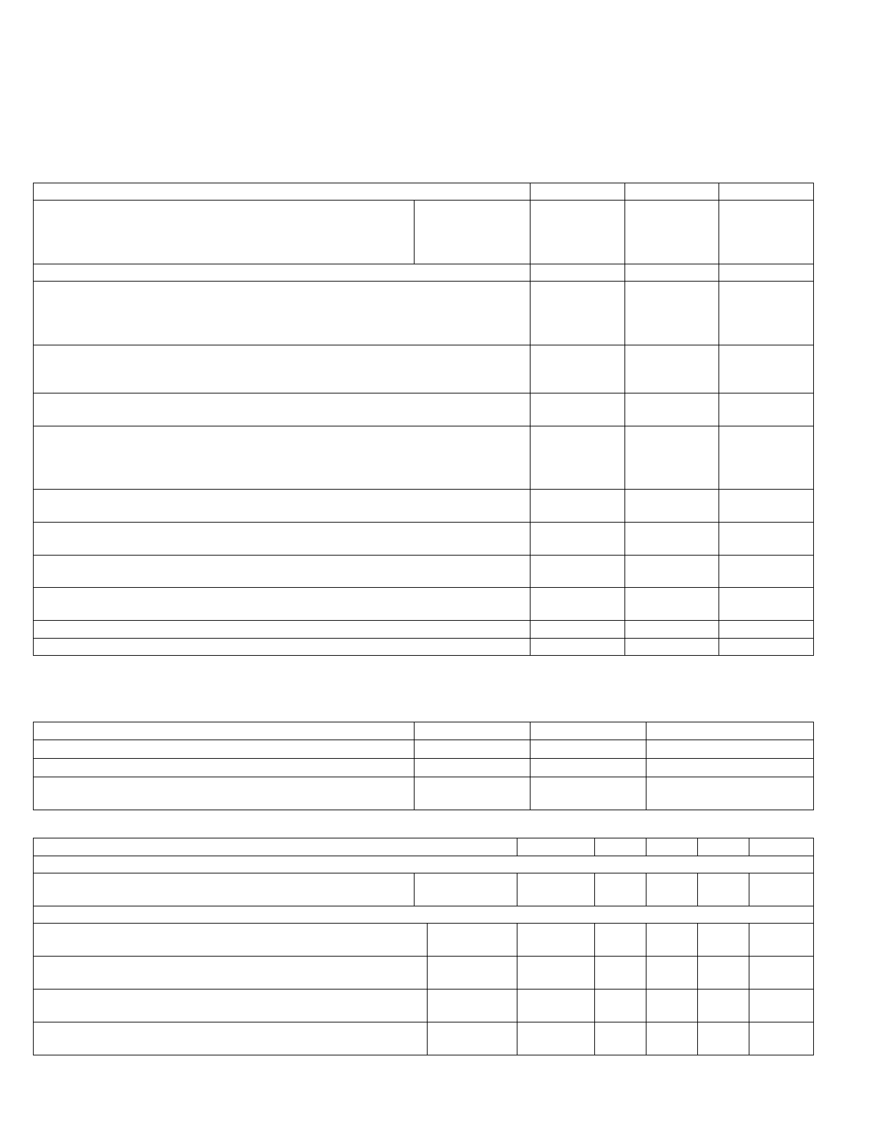
MAXIMUM RATINGS
Rating
Symbol
Value
Unit
2N5060
30
Peak repetitive off-state voltage (1)
2N5061
VDRM
60
V
(TJ = -40 to +110°C, sine wave, 50 to 60 Hz, gate open)
2N5062
VRRM
100
2N5064
200
On-state current RMS (180° conduction angles, TC = 80°C)
Average on-state current
(180° conduction angles)
(TC = 67°C)
(TC = 102°C)
Peak non-repetitive surge current
(TA = 25°C)
(1/2 cycle, sine wave, 60Hz)
IT(RMS)
0.8
A
IT(AV)
0.51
A
0.255
ITSM
10
A
Circuit fusing considerations
(t = 8.3 ms)
I2t
0.4
A2s
Average on-state current
(180° conduction angles)
(TC = 67°C)
(TC = 102°C)
IT(AV)
0.51
A
0.255
Forward peak gate power
(Pulse width ≤ 1.0µsec; TA = 25°C)
PGM
0.1
W
Forward average gate power
(TA = 25°C, t = 8.3ms)
PG(AV)
0.01
W
Forward peak gate current
(Pulse width ≤ 1.0µsec; TA = 25°C)
IGM
1.0
A
Reverse peak gate voltage
(Pulse width ≤ 1.0µsec; TA = 25°C)
VRGM
5.0
V
Operating junction temperature range
TJ
-40 to +110
°C
Storage temperature range
Tstg
-40 to +150
°C
Maximum ratings are those values beyond which device damage can occur. Maximum ratings applied to the device are individual stress limit values (not normal operating conditions) and are not
valid simultaneously. If these limits are exceeded, device functional operation is not implied, damage may occur and reliability may be affected.
1. VDRM and VRRM for all types can be applied on a continuous basis. Ratings apply for zero or negative gate voltage; however, positive gate voltage shall not be applied concurrent with
negative potential on the anode. Blocking voltages shall not be tested with a constant current source such that the voltage ratings of the devices are exceeded.
THERMAL CHARACTERISTICS
Characteristics
Thermal resistance, junction to case
Thermal resistance, junction to ambient
Lead solder temperature
(lead length ≥ 1/16” from case, 10 s max.)
Symbol
RθJC
RθJA
-
Max
75
200
230
Unit
°C/W
°C/W
°C
ELECTRICAL CHARACTERISTICS (TC = 25°C unless otherwise noted)
Characteristics
Symbol
OFF CHARACTERISTICS
Peak repetitive forward or reverse blocking current (2)
(VAK = Rated VDRM or VRRM)
TC = 25°C
TC = 110°C
IDRM, IRRM
ON CHARACTERISTICS
Peak forward on-state voltage (3)
(ITM = 1.2 A peak @ TA = 25°C)
Gate trigger current (continuous DC) (4)
(VAK = 7.0 Vdc, RL = 100 Ω)
Gate trigger voltage (continuous DC) (4)
(VAK = 7.0 Vdc, RL = 100 Ω)
VTM
TC = 25°C
TC = -40°C
IGT
TC = 25°C
TC = -40°C
VGT
Gate non-trigger voltage
(VAK = rated VDRM, RL = 100 Ω) TC = 110°C
VGD
144 Market Street
Kenilworth NJ 07033 USA
phone +1.908.245-7200
fax +1.908.245-0555
Min
-
-
Typ
-
-
Max
10
50
Unit
µA
-
-
1.7
V
-
-
-
-
200
350
µA
-
-
0.8
V
-
-
1.2
0.1
-
-
V
sales@digitroncorp.com
www.digitroncorp.com
Rev. 20130116
Share Link: 