SPT9693 Просмотр технического описания (PDF) - Signal Processing Technologies
Номер в каталоге
Компоненты Описание
производитель
SPT9693 Datasheet PDF : 10 Pages
| |||

TIMING INFORMATION
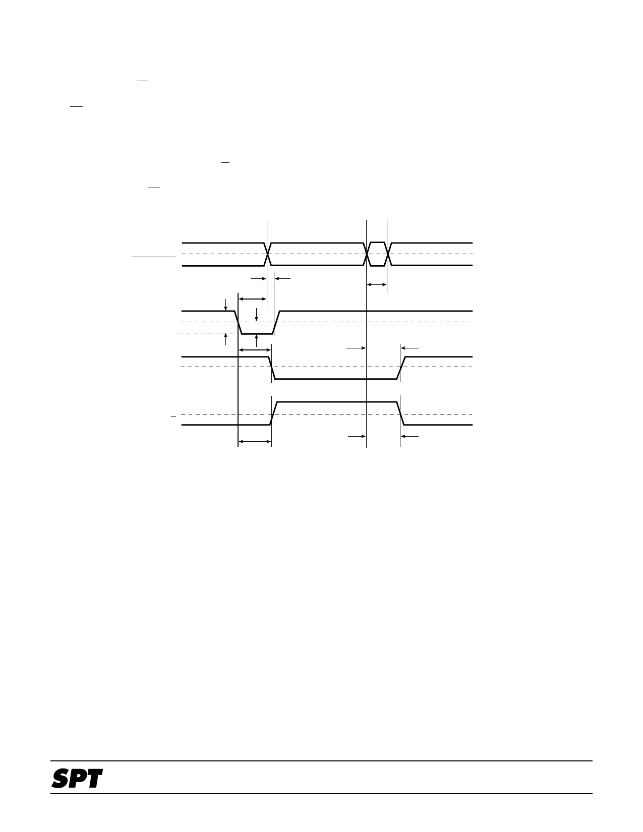
The timing diagram for the comparator is shown in figure
4. If LE is high and LE low in the SPT9693, the comparator
tracks the input difference voltage. When LE is driven low
and LE high, the comparator outputs are latched into their
existing logic states.
The leading edge of the input signal (which consists of a
150 mV overdrive voltage) changes the comparator out-
put after a time of tpdL or tpdH (Q or Q). The input signal
must be maintained for a time tS (set-up time) before the
LE falling edge and LE rising edge and held for time tH
after the falling edge for the comparator to accept data.
After tH, the output ignores the input status until the latch
is strobed again. A minimum latch pulse width of tpL is
needed for strobe operation, and the output transitions
occur after a time of tpLOH or tpLOL.
The set-up and hold times are a measure of the time
required for an input signal to propagate through the first
stage of the comparator to reach the latching circuitry.
Input signals occurring before tS will be detected and held;
those occurring after tH will not be detected. Changes
between tS and tH may not be detected.
Figure 4 – Timing Diagram
Latch Enable
Latch Enable
Differential
Input Voltage
Output Q
tH
tS
VOD
VIN
tpdL
tpL
tpLOH
50%
VRef ±VOS
50%
Output Q
tpdH
t pLOL
50%
VIN+ = 300 mV, VOD = 150 mV
SWITCHING TERMS (Refer to figure 4)
tpdH INPUT TO OUTPUT HIGH DELAY – The propaga-
tion delay measured from the time the input signal
reaches the reference voltage (± the input offset
voltage) to the 50% point of an output LOW to HIGH
transition.
tpdL INPUT TO OUTPUT LOW DELAY – The propaga-
tion delay measured from the time the input signal
reaches the reference voltage (± the input offset
voltage) to the 50% point of an output HIGH to LOW
transition.
tpLOH LATCH ENABLE TO OUTPUT HIGH DELAY – The
propagation delay measured from the 50% point of
the Latch Enable signal LOW to HIGH transition to
50% point of an output LOW to HIGH transition.
tH MINIMUM HOLD TIME – The minimum time after
the negative transition of the Latch Enable signal
that the input signal must remain unchanged in order
to be acquired and held at the outputs.
tpL MINIMUM LATCH ENABLE PULSE WIDTH – The
minimum time that the Latch Enable signal must be
HIGH in order to acquire an input signal change.
tS MINIMUM SET-UP TIME – The minimum time
before the negative transition of the Latch Enable
signal that an input signal change must be present in
order to be acquired and held at the outputs.
VOD VOLTAGE OVERDRIVE – The difference between
the differential input and reference input voltages.
tpLOL LATCH ENABLE TO OUTPUT LOW DELAY – The
propagation delay measured from the 50% point of
the Latch Enable signal LOW to HIGH transition to
the 50% point of an output HIGH to LOW transition.
SPT
8
SPT9693
3/1/01