SPT9693 Просмотр технического описания (PDF) - Signal Processing Technologies
Номер в каталоге
Компоненты Описание
производитель
SPT9693 Datasheet PDF : 10 Pages
| |||
ABSOLUTE MAXIMUM RATINGS (Beyond which damage may occur)1 25 °C
Supply Voltages (Measured to GND)
Positive Supply Voltage (AVCC) ............ –0.5 to +11.0 V
Negative Supply Voltage (AVEE) ........... –11.0 to +0.5 V
Input Voltages
Input Common Mode Voltage ................ –6 to +AVCC+1
Differential Input Voltage .................... –12.0 to +12.0 V
Input Voltage, Latch Controls ...................... –6 to 0.5 V
VIN to AVCC Differential Voltage ............... –16 to +1.0 V
VIN to AVEE Differential Voltage ............... +4 to +21.0 V
Output
Output Current ................................................... 30 mA
Temperature
Operating Temperature, ambient ................ 0 to +70 °C
junction......................+150 °C
Lead Temperature, (soldering 60 seconds) ..... +300 °C
Storage Temperature ............................ –65 to +150 °C
Note: 1. Operation at any Absolute Maximum Rating is not implied. See
Electrical Specifications for proper nominal applied conditions
in typical applications. Application of multiple maximum rating
conditions at the same time may damage the device.
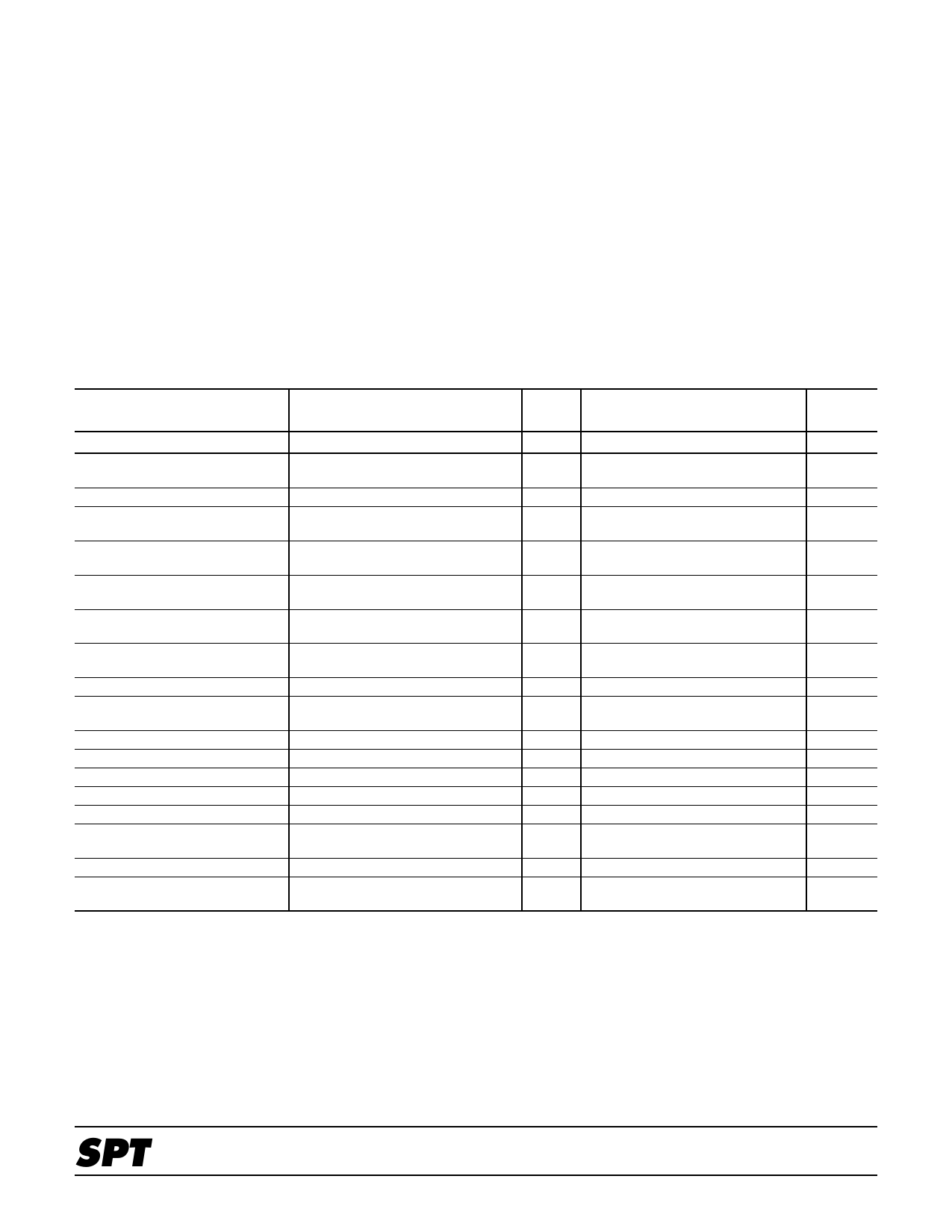
ELECTRICAL SPECIFICATIONS
TA = +25 °C, AVCC = +10 V, AVEE = –10.0 V, RL = 50 Ohm to –2 V, unless otherwise specified.
PARAMETERS
TEST
CONDITIONS
TEST
LEVEL
MIN
DC CHARACTERISTICS
Input Offset Voltage
VIN (Common Mode) = 0
I
TMIN<TA<TMAX
IV
Offset Voltage Tempco
V
Input Bias Current
Input Bias Current
TMIN<TA<TMAX
I
VIN (Common Mode) = –3 to +7 V
TMIN<TA<TMAX
I
VIN (Common Mode) = +7 to +8 V
Input Offset Current
V
TMIN<TA<TMAX
V
Positive Supply Current (Dual) AVCC=10 V
I
Negative Supply Current (Dual) AVEE=–10.0 V
I
Positive Supply Voltage, AVCC
IV
Negative Supply Voltage, AVEE
IV
Input Common Mode Range
I
Latch Enable
Common Mode Range
IV
Differential Voltage Range
I
Open Loop Gain
V
Differential Input Resistance
V
Input Capacitance
V
Power Supply Sensitivity
V
Common Mode Rejection Ratio
I
TMIN<TA<TMAX
IV
Power Dissipation
Dual
I
Output High Level
ECL 50 Ohms to –2 V
I
Output Low Level
ECL 50 Ohms to –2 V
I
–25
–25
9.75
–9.75
–3.0
–2.0
50
45
–.98
–1.95
TYP
MAX
0.0
0.0
50
±10
±50
±1.0
±10
3
40
10.0
–10.0
52
2
1.0
60
60
55
430
+25
+25
±100
±150
6
55
10.25
–10.25
+8.0
0
±10
610
–.70
–1.65
UNITS
mV
mV
µV/°C
nA
nA
nA
nA
mA
mA
V
V
V
V
V
dB
GΩ
pF
dB
dB
dB
mW
V
V
SPT
2
SPT9693
3/1/01
Share Link: 