HLMP-3600 Просмотр технического описания (PDF) - Avago Technologies
Номер в каталоге
Компоненты Описание
производитель
HLMP-3600
Avago Technologies

HLMP-3600 Datasheet PDF : 8 Pages
| |||
Precautions
Lead Forming
• The leads of an LED lamp may be preformed or cut to
length prior to insertion and soldering into PC board.
• If lead forming is required before soldering, care must
be taken to avoid any excessive mechanical stress
induced to LED package. Otherwise, cut the leads
of LED to length after soldering process at room
temperature. The solder joint formed will absorb the
mechanical stress of the lead cutting from traveling to
the LED chip die attach and wirebond.
• It is recommended that tooling made to precisely form
and cut the leads to length rather than rely upon hand
operation.
Soldering Conditions
• Care must be taken during PCB assembly and soldering
process to prevent damage to LED component.
• The closest LED is allowed to solder on board is 1.59
mm below the body (encapsulant epoxy) for those
parts without standoff.
• Recommended soldering conditions:
Pre-heat Temperature
Pre-heat Time
Peak Temperature
Dwell Time
Wave Soldering
105°C Max.
30 sec Max.
250°C Max.
3 sec Max.
Manual Solder
Dipping
–
–
260°C Max.
5 sec Max.
• Wave soldering parameter must be set and maintained
according to recommended temperature and dwell
time in the solder wave. Customer is advised to
periodically check on the soldering profile to ensure
the soldering profile used is always conforming to
recommended soldering condition.
• If necessary, use fixture to hold the LED component
in proper orientation with respect to the PCB during
soldering process.
• Proper handling is imperative to avoid excessive
thermal stresses to LED components when heated.
Therefore, the soldered PCB must be allowed to cool to
room temperature, 25°C, before handling.
• Special attention must be given to board fabrication,
solder masking, surface plating and lead holes size and
component orientation to assure solderability.
• Recommended PC board plated through hole sizes for
LED component leads:
LED Component
Lead Size
Diagonal
Plated Through-
Hole Diameter
Lead size (typ.) 0.45 × 0.45 mm 0.636 mm 0.98 to 1.08 mm
(0.018 × 0.018 in.) (0.025 in) (0.039 to 0.043 in)
Dambar shear- 0.65 mm
off area (max.) (0.026 in)
0.919 mm
(0.036 in)
Lead size (typ.) 0.50 × 0.50 mm 0.707 mm 1.05 to 1.15 mm
(0.020 × 0.020 in.) (0.028 in) (0.041 to 0.045 in)
Dambar shear- 0.70 mm
off area (max.) (0.028 in)
0.99 mm
(0.039 in)
Note: Refer to application note AN1027 for more information on
soldering LED components.
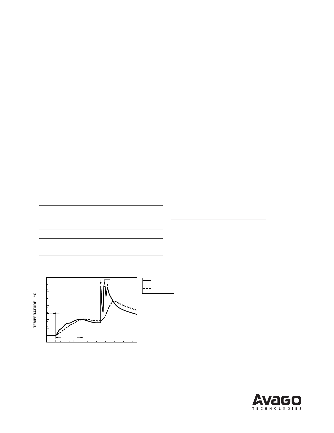
TURBULENT WAVE
250
200
LAMINAR WAVE
HOT AIR KNIFE
BOTTOM SIDE
OF PC BOARD
TOP SIDE OF
PC BOARD
150
FLUXING
100
50
30
PREHEAT
CONVEYOR SPEED = 1.83 M/MIN (6 FT/MIN)
PREHEAT SETTING = 150°C (100°C PCB)
SOLDER WAVE TEMPERATURE = 245°C
AIR KNIFE AIR TEMPERATURE = 390°C
AIR KNIFE DISTANCE = 1.91 mm (0.25 IN.)
AIR KNIFE ANGLE = 40°
SOLDER: SN63; FLUX: RMA
NOTE: ALLOW FOR BOARDS TO BE
SUFFICIENTLY COOLED BEFORE EXERTING
MECHANICAL FORCE.
0 10 20 30 40 50 60 70 80 90 100
TIME – SECONDS
Figure 9. Recommended wave soldering profile.
For product information and a complete list of distributors, please go to our web site: www.avagotech.com
Avago, Avago Technologies, and the A logo are trademarks of Avago Technologies in the United States and other countries.
Data subject to change. Copyright © 2005-2013 Avago Technologies. All rights reserved.
AV02-0379EN - June 7, 2013
Share Link: