DJLXT908LC Просмотр технического описания (PDF) - Intel
Номер в каталоге
Компоненты Описание
производитель
DJLXT908LC Datasheet PDF : 44 Pages
| |||
LXT908 — Universal 3.3V 10BASE-T and AUI Transceiver
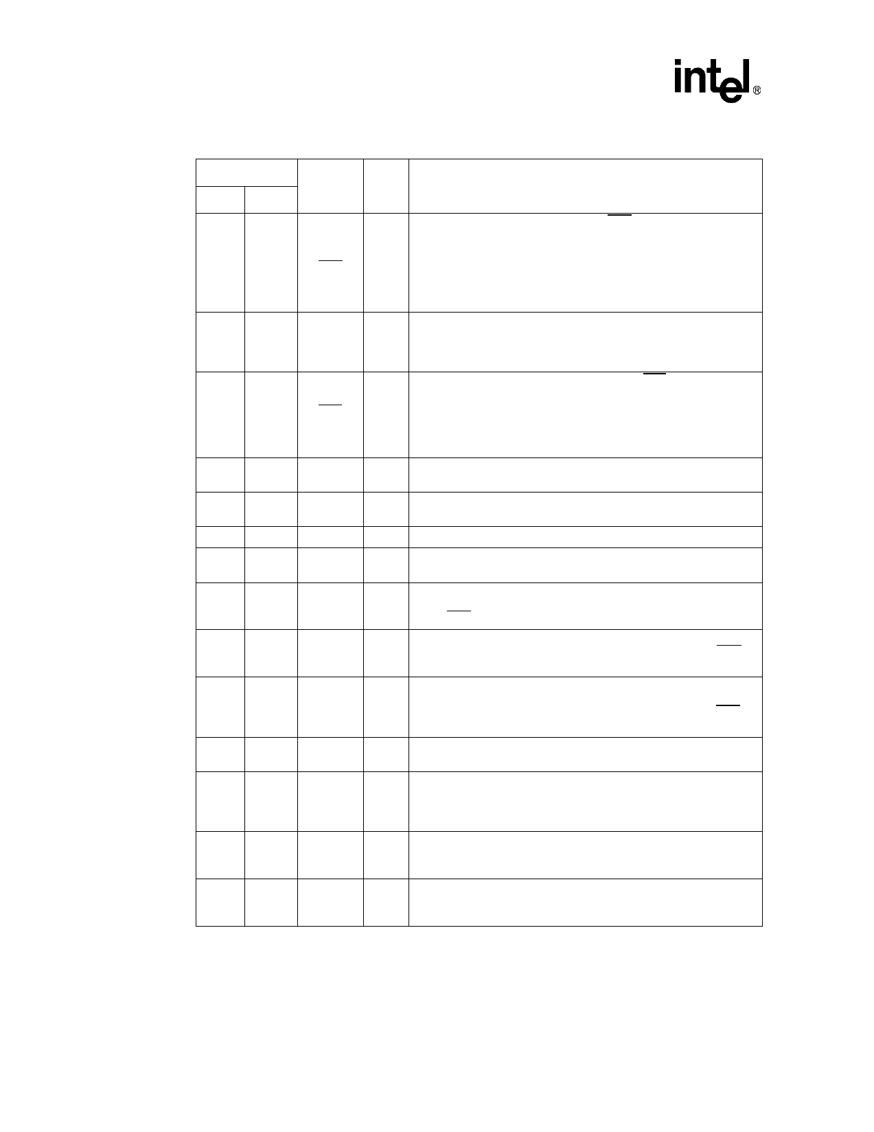
Table 1. LXT908 Signal Descriptions (Continued)
Pin#
PLCC LQFP
Symbol
19
35
LEDT/
PDN
20
36
LEDL
LEDC/
21
37
FDE
22
38
LBK
23
39
GND1
33
55
GND2
–
40
GNDA
24
42
RBIAS
26
45
RXD
27
46
CD
28
47
RCLK
30
52
PLR
32
54
TPOPA
35
57
TPONA
31
53
TPOPB
36
58
TPONB
37
59
DSQE
3839
61
62
TPIP
TPIN
I/O
Description
Transmit LED (LEDT)/Power Down (PDN). Open drain driver for
the transmit indicator LED. Output is pulled Low during transmit. Do
O
I
not allow this pin to float. If unused, tie High. LED “On” time
(Low output) is extended by approximately 100 ms. If externally tied
Low, the LXT908 goes to power-down state. In power-down state,
TCLK, COL, RXD, CD, and RCLK (pins 11, 16, 26, 27, and 28,
respectively) are tri-stated.
Link LED. Open drain driver for link integrity indicator LED. Output
O is pulled Low during link test pass. If externally tied Low, internal
I circuitry is forced to “Link Pass” state and the LXT908 will continue
to transmit link test pulses.
Collision LED (LEDC)/Full Duplex Enable (FDE). Open drain
driver for the collision indicator LED pulls Low during collision. LED
O “On” time (Low output) is extended by approximately 100 ms. If
I externally tied Low, the LXT908 disables the internal TP loopback
and collision detection circuits to allow full-duplex operation or
external twisted-pair loopback.
I
Loopback. Enables internal loopback mode. Refer to Functional
Description and Test Specifications for details.
– Ground Returns 1 and 2. Connect to negative power supply
– terminal (ground).
– Analog Ground. Ground for analog plane.
I
Bias Control. A 12.4 kΩ 1% resistor to ground at this pin controls
operating circuit bias.
Receive Data. Output signal connected directly to the receive data
O input of the controller. RXD goes to high impedance (tri-state) when
LEDT/PDN is pulled Low externally.
Carrier Detect. An output to notify the controller of activity on the
O network. CD goes to high impedance (tri-state) when LEDT/PDN is
pulled Low externally.
Receive Clock. A recovered 10 MHz clock that is synchronous to
O
the received data and connected to the controller receive clock
input. RCLK goes to high impedance (tri-state) when LEDT/PDN is
pulled Low externally.
O
Polarity Reverse. Output goes High to indicate reversed polarity at
the TP input.
O Twisted-Pair Transmit Pairs A & B. Two differential driver pair
O outputs (A and B) to the twisted-pair cable. The outputs are pre-
O equalized. Each pair must be shorted together with an 11.5 Ω 1%
O resistor to match an impedance of 100Ω.
Disable SQE. When DSQE is High, the SQE function is disabled.
I When DSQE is Low, the SQE function is enabled. SQE must be
disabled for normal operation in Hub/Switch applications.
I
I
Twisted-Pair Receive Pair. A differential input pair from the TP
cable. Receive filter is integrated on chip. No external filters are
required.
10
Datasheet
Document #: 249049
Revision #: 002
Rev. Date: June 19, 2001
Share Link: 