FM24CL64B-GA(2011) Просмотр технического описания (PDF) - Ramtron International Corporation
Номер в каталоге
Компоненты Описание
производитель
FM24CL64B-GA Datasheet PDF : 12 Pages
| |||
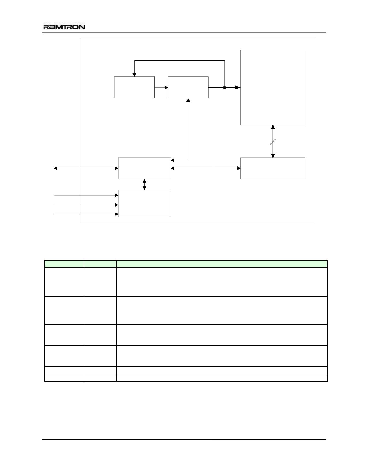
FM24CL64B - 64Kb 3V I2C F-RAM (Automotive Temp.)
Counter
Address
Latch
1K x 64
FRAM Array
SDA
SCL
WP
A0-A2
Serial to Parallel
Converter
Control Logic
8
Data Latch
Figure 1. FM24CL64B Block Diagram
Pin Description
Pin Name
A0-A2
Type
Input
SDA
I/O
SCL
WP
VDD
VSS
Input
Input
Supply
Supply
Pin Description
Device Select Address 0-2: These pins are used to select one of up to 8 devices of
the same type on the same two-wire bus. To select the device, the address value on
the two pins must match the corresponding bits contained in the slave address. The
address pins are pulled down internally.
Serial Data/Address: This is a bi-directional pin for the two-wire interface. It is
open-drain and is intended to be wire-OR‟d with other devices on the two-wire bus.
The input buffer incorporates a Schmitt trigger for noise immunity and the output
driver includes slope control for falling edges. An external pull-up resistor is
required.
Serial Clock: The serial clock pin for the two-wire interface. Data is clocked out of
the part on the falling edge, and into the device on the rising edge. The SCL input
also incorporates a Schmitt trigger input for noise immunity.
Write Protect: When tied to VDD, addresses in the entire memory map will be write-
protected. When WP is connected to ground, all addresses may be written. This pin
is pulled down internally.
Supply Voltage
Ground
Rev. 1.1
June 2011
Page 2 of 12
Share Link: 