A54SX08A Просмотр технического описания (PDF) - Actel Corporation
Номер в каталоге
Компоненты Описание
производитель
A54SX08A Datasheet PDF : 108 Pages
| |||
SX-A Family FPGAs
Clock Resources
Actel’s high-drive routing structure provides three clock
networks (Table 1-1). The first clock, called HCLK, is
hardwired from the HCLK buffer to the clock select
multiplexor (MUX) in each R-cell. HCLK cannot be
connected to combinatorial logic. This provides a fast
propagation path for the clock signal. If not used, this
pin must be set as Low or High on the board. It must not
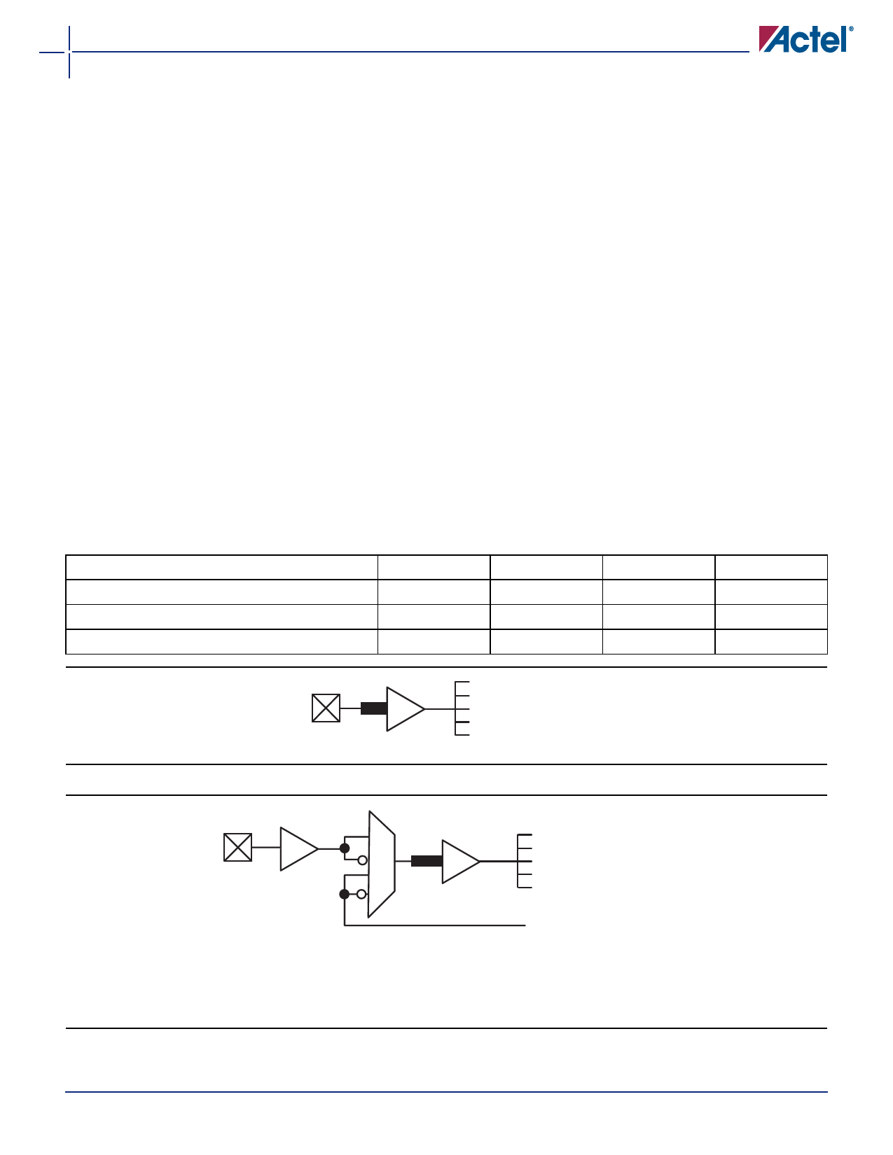
be left floating. Figure 1-7 describes the clock circuit
used for the constant load HCLK and the macros
supported.
HCLK does not function until the fourth clock cycle each
time the device is powered up to prevent false output
levels due to any possible slow power-on-reset signal and
fast start-up clock circuit. To activate HCLK from the first
cycle, the TRST pin must be reserved in the Design
software and the pin must be tied to GND on the board.
Two additional clocks (CLKA, CLKB) are global clocks that
can be sourced from external pins or from internal logic
signals within the SX-A device. CLKA and CLKB may be
connected to sequential cells or to combinational logic. If
CLKA or CLKB pins are not used or sourced from signals,
these pins must be set as Low or High on the board. They
must not be left floating. Figure 1-8 describes the CLKA
and CLKB circuit used and the macros supported in SX-A
devices with the exception of A54SX72A.
In addition, the A54SX72A device provides four
quadrant clocks (QCLKA, QCLKB, QCLKC, and QCLKD—
corresponding to bottom-left, bottom-right, top-left,
and top-right locations on the die, respectively), which
can be sourced from external pins or from internal logic
signals within the device. Each of these clocks can
individually drive up to an entire quadrant of the chip,
or they can be grouped together to drive multiple
quadrants (Figure 1-9 on page 1-6). QCLK pins can
function as user I/O pins. If not used, the QCLK pins
must be tied Low or High on the board and must not be
left floating.
For more information on how to use quadrant clocks in
the A54SX72A device, refer to the Global Clock Networks
in Actel’s Antifuse Devices and Using A54SX72A and
RT54SX72S Quadrant Clocks application notes.
The CLKA, CLKB, and QCLK circuits for A54SX72A as well
as the macros supported are shown in Figure 1-10 on
page 1-6. Note that bidirectional clock buffers are only
available in A54SX72A. For more information, refer to
the "Pin Description" section on page 1-15.
Table 1-1 • SX-A Clock Resources
A54SX08A
A54SX16A
A54SX32A
A54SX72A
Routed Clocks (CLKA, CLKB)
2
2
2
2
Hardwired Clocks (HCLK)
1
1
1
1
Quadrant Clocks (QCLKA, QCLKB, QCLKC, QCLKD)
0
0
0
4
Figure 1-7 • SX-A HCLK Clock Buffer
HCLKBUF
Constant Load
Clock Network
Figure 1-8 • SX-A Routed Clock Buffer
CLKBUF
CLKBUFI
CLKINT
CLKINTI
Clock Network
From Internal Logic
v5.3
1-5
Share Link: 