FAN102 Просмотр технического описания (PDF) - Fairchild Semiconductor
Номер в каталоге
Компоненты Описание
производитель
FAN102 Datasheet PDF : 16 Pages
| |||
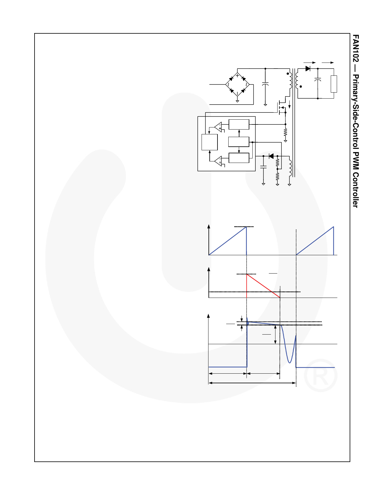
Functional Description
Figure 24 shows the basic circuit diagram of primary-
side regulated flyback converter with typical waveforms
shown in Figure 25. Generally, discontinuous
conduction mode (DCM) operation is preferred for
primary-side regulation since it allows better output
regulation. The operation principles of DCM flyback
converter are as follows:
During the MOSFET ON time (tON), input voltage (VDL) is
applied across the primary-side inductor (Lm). Then
MOSFET current (Ids) increases linearly from zero to the
peak value (Ipk). During this time, the energy is drawn
from the input and stored in the inductor.
When the MOSFET is turned off, the energy stored in
the inductor forces the rectifier diode (D) to turn on.
While the diode is conducting, the output voltage (Vo),
together with diode forward voltage drop (VF), are
applied across the secondary-side inductor (Lm×Ns2/
Np2) and the diode current (ID) decreases linearly from
the peak value (Ipk×Np/Ns) to zero. At the end of inductor
current discharge time (tDIS), all the energy stored in the
inductor has been delivered to the output.
When the diode current reaches zero, the transformer
auxiliary winding voltage (VW) begins to oscillate by the
resonance between the primary-side inductor (Lm) and
the effective capacitor loaded across MOSFET.
During the inductor current discharge time, the sum of
output voltage and diode forward voltage drop is
reflected to the auxiliary winding side as (VO+VF)×
NA/NS. Since the diode forward voltage drop decreases
as current decreases, the auxiliary winding voltage
reflects the output voltage best at the end of diode
conduction time where the diode current diminishes to
zero. By sampling the winding voltage at the end of the
diode conduction time, the output voltage information
can be obtained. The internal error amplifier for output
voltage regulation (EA_V) compares the sampled
voltage with internal precise reference to generate error
voltage (VCOMV), which determines the duty cycle of the
MOSFET in CV mode.
Meanwhile, the output current can be estimated using
the peak drain current and inductor current discharge
time since output current is same as average of the
diode current in steady state.
The output current estimator picks up the peak value of
the drain current with a peak detection circuit and
calculates the output current using the inductor
discharge time (tDIS) and switching period (tS). The
output information is compared with internal precise
reference to generate error voltage (VCOMI), which
determines the duty cycle of the MOSFET in CC mode.
Among the two error voltages, VCOMV and VCOMI, the
smaller actually determines the duty cycle. During
constant voltage regulation mode, VCOMV determines the
duty cycle while VCOMI is saturated to high. During
constant current regulation mode, VCOMI determines the
duty cycle while VCOMV is saturated to HIGH.
VAC
+
V DL
-
Np:Ns
ID
D
Lm
+ VF -
Io
+
L
VO
O
A
D
-
Gate
Ids
EA_I
VCOMI
Ref
PWM
Control
Io
Estimator
t DIS
Detector
CS
RCS
VS
V COMV
Vo
VDD
NA
EA_V
Estimator
Ref
RS1
+
Vw
Primary-Side Regulation
RS2
-
Controller
Figure 24. Simplified PSR Flyback Converter Circuit
Ids (MOSFET Drain-to-Source Current)
I pk
ID (Diode Current)
I
pk
•
NP
NS
V (Auxiliary Winding Voltage)
W
VF•
NA
NS
VO •
NA
NS
I D.avg = I o
t
ON
t
DIS
tS
Figure 25. Key Waveforms of DCM Flyback
Converter
© 2008 Fairchild Semiconductor Corporation
FAN102 Rev. 1.0.3
10
www.fairchildsemi.com
Share Link: 