AD636K Просмотр технического описания (PDF) - Analog Devices
Номер в каталоге
Компоненты Описание
производитель
AD636K Datasheet PDF : 16 Pages
| |||
AD636
Data Sheet
APPLICATIONS
The input and output signal ranges are a function of the supply
voltages as detailed in the specifications. The AD636 can also be
used in an unbuffered voltage output mode by disconnecting the
input to the buffer. The output then appears unbuffered across
the 10 kΩ resistor. The buffer amplifier can then be used for
other purposes. Further, the AD636 can be used in a current
output mode by disconnecting the 10 kΩ resistor from the ground.
The output current is available at Pin 8 (Pin 10 on the H package)
with a nominal scale of 100 μA per volt rms input, positive out.
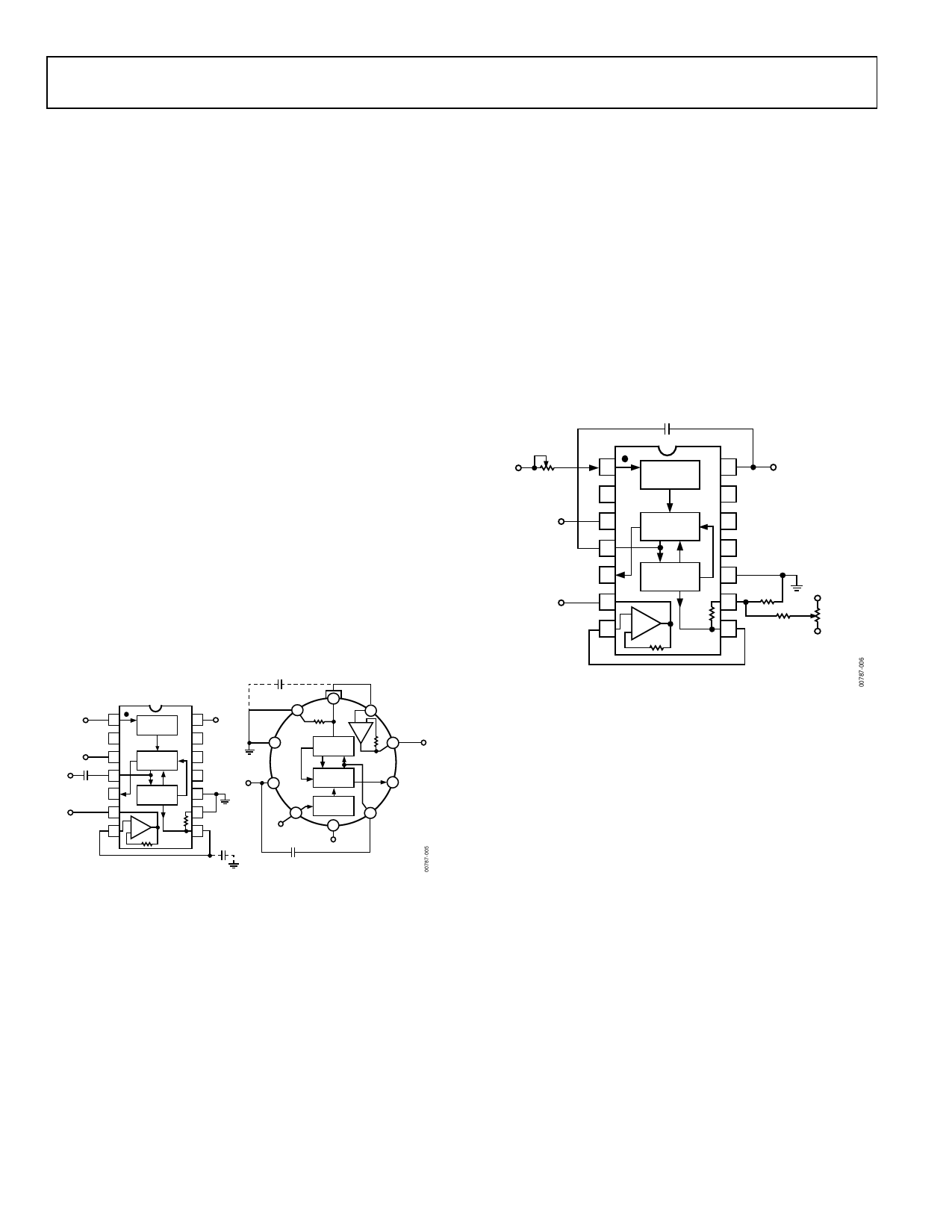
STANDARD CONNECTION
The AD636 is simple to connect for the majority of high accuracy
rms measurements, requiring only an external capacitor to set
the averaging time constant. The standard connection is shown
in Figure 9 In this configuration, the AD636 measures the rms
of the ac and dc level present at the input but shows an error for
low frequency inputs as a function of the filter capacitor, CAV, as
shown in Figure 13. Therefore, if a 4 μF capacitor is used, the
additional average error at 10 Hz is 0.1%, and at 3 Hz it is 1%.
The accuracy at higher frequencies is according to specification.
If it is desired to reject the dc input, a capacitor is added in
series with the input, as shown in Figure 11; the capacitor must
be nonpolar. If the AD636 is driven with power supplies with a
considerable amount of high frequency ripple, it is advisable to
bypass both supplies to ground with 0.1 μF ceramic discs as near
the device as possible. CF is an optional output ripple filter.
CF
(OPTIONAL)
IOUT
VIN
erms
1
ABSOLUTE
VALUE
NC 2 AD636
–VS
–V
3
SQUARER
CAV
+V + C –
4
dB 5
BUF OUT
6
DIVIDER
CURRENT
MIRROR
BUF IN
7
+
BUF
–
10kΩ
10kΩ
+VS
14
+V
13 NC
12 NC
RL
1
10
10kΩ
9 BUF IN
COM AD636
+BUF–
BUF OUT
2
CURRENT
MIRROR
8
VOUT
10kΩ
11 NC
COM
10
+VS
+V
3
RL
9
IOUT
8
CF
(OPTIONAL)
VIN 4
erms
+–
SQUARER
DIVIDER
ABSOLUTE
VALUE
5
–VS
–V
7 dB
6
CAV
CAV
NC = NO CONNECT
Figure 9. Standard RMS Connection
OPTIONAL TRIMS FOR HIGH ACCURACY
If it is desired to improve the accuracy of the AD636, the
external trims shown in Figure 10 can be added. R4 is used to
trim the offset. The scale factor is trimmed by using R1 as
shown. The insertion of R2 allows R1 to either increase or
decrease the scale factor by ±1.5%.
The trimming procedure is as follows:
• Ground the input signal, VIN, and adjust R4 to give 0 V
output from Pin 6. Alternatively, R4 can be adjusted to give
the correct output with the lowest expected value of VIN.
• Connect the desired full-scale input level to VIN, either dc or a
calibrated ac signal (1 kHz is the optimum frequency); then
trim R1 to give the correct output from Pin 6, that is, 200 mV
dc input should give 200 mV dc output. Of course, a ±200 mV
peak-to-peak sine wave should give a 141.4 mV dc output.
The remaining errors, as given in the specifications, are due to
the nonlinearity.
SCALE
FACTOR
ADJUST
erms
R1
200Ω
±1.5%
–V
CAV
–+
VIN
1
NC 2
–VS
3
CAV
4
ABSOLUTE
VALUE
AD636
SQUARER
DIVIDER
+VS
14
+V
13 NC
12 NC
11 NC
dB 5
BUF OUT
6
VOUT
BUF IN
7
CURRENT
MIRROR
+
BUF
–
10kΩ
10kΩ
COM
10
R2
RL 154Ω
+VS
9
R4
8
IOUT R3
470kΩ
500kΩ
–VS
OFFSET
ADJUST
NC = NO CONNECT
Figure 10. Optional External Gain and Output Offset Trims
SINGLE-SUPPLY CONNECTION
Although the applications illustrated in Figure 9 and Figure 10
assume the use of dual power supplies, three external bias
components connected to the COM pin enable powering the
AD636 with unipolar supplies as low as 5 V. The two resistors
and capacitor network shown connected to Pin 10 in Figure 11
are satisfactory over the same range of voltages permissible with
dual supply operation. Any external bias voltage applied to Pin 10 is
internally reflected to the VIN pin, rendering the same ac operation
as with a dual supply. DC or ac + dc conversion is impractical,
due to the resultant dc level shift at the input. The capacitor
insures that no extraneous signals are coupled into the COM
pin. The values of the resistors are relatively high to minimize
power consumption because only 1 µA of bias current flows
into Pin 10 (Pin 2 on the H package).
Alternately, the COM pin of some CMOS ADCs provides a suitable
artificial ground for the AD636. AC input coupling requires only
Capacitor C2 as shown; a dc return is not necessary because it is
provided internally. C2 is selected for the proper low frequency
break point with the input resistance of 6.7 kΩ; for a cut-off at
10 Hz, C2 should be 3.3 μF. The signal ranges in this connection are
Rev. E | Page 10 of 16
Share Link: 