THC63LVD104S Просмотр технического описания (PDF) - THine Electronics, Inc.
Номер в каталоге
Компоненты Описание
производитель
THC63LVD104S Datasheet PDF : 12 Pages
| |||
THC63LVD104S Rev.1.0
THC63LVD104S
112MHz 30Bits Color LVDS Receiver
General Description
The THC63LVD104S receiver is designed to support
pixel data transmission between Host and Flat Panel
Display from NTSC up to SXGA resolutions. The
THC63LVD104S converts the LVDS data streams back
into 35bits of CMOS/TTL data with rising edge or fall-
ing edge clock for convenient with a variety of LCD
panel controllers.At a transmit clock frequency of
112MHz, 30bits of RGB data and 5bits of timing and
control data (HSYNC,VSYNC,DE,CNTL1,CNTL2)
are transmitted at an effective rate of 784Mbps per
LVDS channel.Using a 112MHz clock, the data
throughput is 490Mbytes per second.
Features
• Wide dot clock range: 8-112MHz suited for NTSC,
VGA, SVGA, XGA, and SXGA
• PLL requires no external components
• 50% output clock duty cycle
• TTL clock edge and position programmable(3 step)
• Power down mode
• Low power single 2.5V CMOS design
• TQFP 64pin
• Pin compatible with THC63LVD104A
• Fail-safe for Open CLK Input
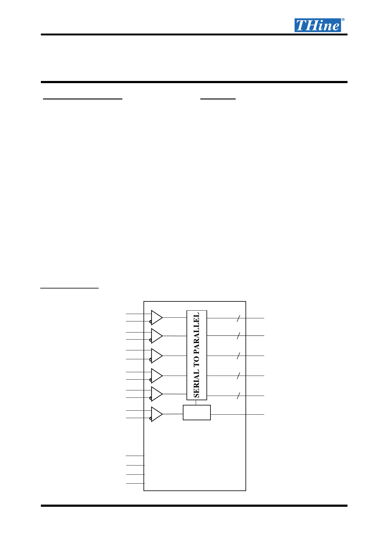
Block Diagram
LVDS INPUT
RA+/-
RB+/-
RC+/-
RD+/-
RE+/-
RCLK+/-
(8 to112MHz)
CMOS/TTL INPUT
R/F
DK
PD
OE
PLL
Copyright 2004 THine Electronics, Inc. All rights reserved
1
CMOS/TTL OUTPUT
7
RA6-RA0
7
RB6-RB0
7
RC6-RC0
7
RD6-RD0
7
RE6-RE0
CLKOUT
THine Electronics, Inc.
Share Link: 