LT1180A –ü—Ä–æ—Å–º–æ—Ç—Ä —Ç–µ—Ö–Ω–∏—á–µ—Å–∫–æ–≥–æ –æ–ø–∏—Å–∞–Ω–∏—è (PDF) - Linear Technology
–ù–æ–º–µ—Ä –≤ –∫–∞—Ç–∞–ª–æ–≥–µ
–ö–æ–º–ø–æ–Ω–µ–Ω—Ç—ã –û–ø–∏—Å–∞–Ω–∏–µ
–ø—Ä–æ–∏–∑–≤–æ–¥–∏—Ç–µ–ª—å
LT1180A Datasheet PDF : 12 Pages
| |||
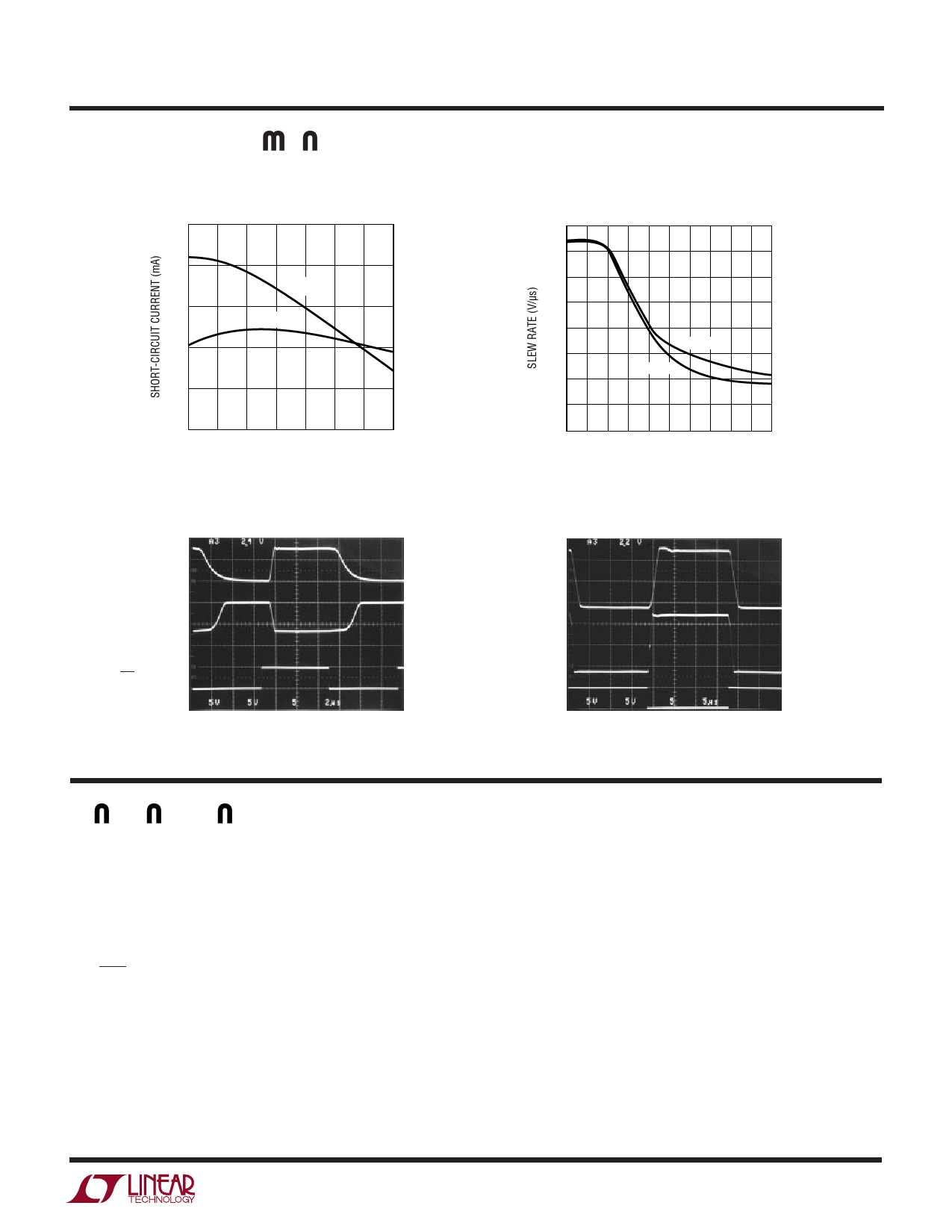
TYPICAL PERFOR A CE CHARACTERISTICS
LT1180A/LT1181A
Receiver Short-Circuit Current
50
40
RX ISC–
30
RX ISC+
20
10
0
–55 –25
0 25 50 75 100 125
TEMPERATURE (°C)
LT1180A • TPC10
Shutdown to Driver Outputs
10V
DRIVER 1 5V
OUTPUT
GND
GND
DRIVER 2 – 5V
OUTPUT
– 10V
ON/OFF PIN
LT1180A • TPC12
Slew Rate vs Load Capacitance
16
14
12
10
8
+SLEW
6
–SLEW
4
2
0
0 0.5 1.0 1.5 2.0 2.5 3.0 3.5 4.0 4.5 5.0
LOAD CAPACITANCE (nF)
LT1180A • TPC11
Driver Output Waveforms
DRIVER OUTPUT
RL = 3k
CL = 2500pF
DRIVER OUTPUT
RL = 3k
INPUT
LT1180A • TPC13
PI FU CTIO S
VCC: 5V Input Supply Pin. This pin should be decoupled
with a 0.1µF ceramic capacitor close to the package pin.
Insufficient supply bypassing can result in low output
drive levels and erratic charge pump operation.
GND: Ground Pin.
ON/OFF: A TTL/CMOS Compatible Operating Mode Con-
trol. A logic low puts the LT1180A in shutdown mode.
Supply current drops to zero and both driver and receiver
outputs assume a high impedance state. A logic high fully
enables the device.
V+: Positive Supply Output (RS232 Drivers). V+ ≈ 2VCC –
1.5V. This pin requires an external charge storage capaci-
tor C ≥ 0.1µF, tied to ground or VCC. Larger value capaci-
tors may be used to reduce supply ripple. With multiple
transceivers, the V+ and V – pins may be paralleled into
common capacitors.
V–: Negative Supply Output (RS232 Drivers). V – ≈ –(2VCC
– 2.5V). This pin requires an external charge storage
capacitor C ≥ 0.1µF. Larger value capacitors may be used
to reduce supply ripple. With multiple transceivers, the V+
and V – pins may be paralleled into common capacitors.
11801afb
5
Share Link: 