LND-TRM34 Просмотр технического описания (PDF) - Linear Dimensions Semiconductor
Номер в каталоге
Компоненты Описание
производитель
LND-TRM34 Datasheet PDF : 6 Pages
| |||
LND TRM34
LOW POWER 300 TO 500 MHz FSK TRANSMITTER
Matching
network and
antenna options
(continued)
Figure 2 shows a typical application diagram.
In order to minimise second harmonic distortion,
a differential output configuration is recom-
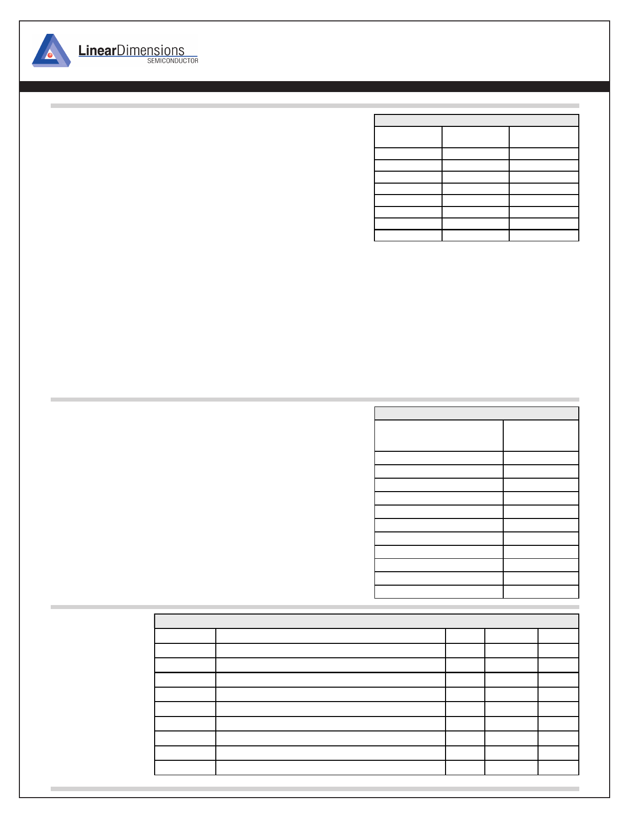
Table 5: Output Power Settings
R
(kOhms)
Output power
(dBm)
Current cons.
(mA)
mended. The LND TRM34 needs the following:
2.8
2
25
1) a dc bias reference to VCC (preferrably through
3.8
0
22
direct connection of a loop antenna connected
5.2
-2
20
to VCC at its centre, or use of printed bias
6.7
-4
19
inductors with a connection to VCC). Linear’s
8.5
-6
18
TRM3x series of evaluation boards provide
9.7
-8
17
large and small loop antenna solutions for cus-
10.3
-10
16
tomers to copy. These boards require a minimum
10.7
-12
16
number of external components, and importantly
no discrete inductors are required. For driving an 3) the PLL synthesizer is designed to operate with
external single-ended antenna, a high efficiency
an external second order loop as shown in
printed balun is also available.
figure 2, with component values as shown in
For optimum operation, the following points are
highlighted:
1) The IC can provide 7.5mA of current into the load
Table 7. These values determine the loop
bandwidth and dynamics and operation of the
loop is not guaranteed for any other values
2) for maximum output power, it is recommended
that the antenna load be transformed to an
impedance of 200Ohms (RPS is set at
3.9kOhms)
4) The bias current for the power amplifier directly
controls the output current and hence the O/P
power. This bias current is set by an external
resistor connected between PS and ground.
Output power versus RI values is shown in
Table 5, for a differential load impedance of 200 Ω.
Frequency
deviation
External
components
The amount of frequency deviation depends
upon the type of external crystal used. An on-
chip capacitor of 3pF is switched in parallel
with the crystal to shift its frequency of operation.
For instance, on the TRM3x series of evalua-
tion boards, the peak-to-peak frequency
deviation possible with the supplied crystal is
over 15kHz in SOP packaged parts and 25 kHz
for SSOP packaged parts. The crystal param-
eters are specified as shown aside:
For smaller frequency deviations, then a less
pullable crystal can be specified (eg 20 pF or
30 pF load crystals are less pullable). If peak-to-
peak frequency deviations of much greater than
15kHz are required, then please consult Linear
Dimensions for information on how to achieve this.
Table 6 - Crystal specifications
Supplier/part number
Frequency
Package
Operating mode
Calibration tolerance
Temperature stability
Operating temp range
Circuit loading
Maximum ESR, R1
Static capacitance (typical), Co
Motional capacitance (typical), C1
Pullability
Euroquartz: B537
Tel.:
0044146076477
6.78 MHz
HC49/U
AT
+/-10 ppm
+/-10 ppm
-10 to + 60°C
10 pF
50 Ohms
5 pF
20 fF
40 ppm/pF
Table 7: Recommended External Components
Component
Function
C1
Crystal Oscillator
C2
Crystal Oscillator
C5
Supply Decoupling
C6
Regulator Decoupling
C7
PLL Loop Filter
C8
PLL Loop Filter
R1
O/P power set
R2
PLL Loop Filter
X1
Crystal
Value
22 pF
22 pF
100
100
1
47
3.9
3.3
6.78
Tolerance
± 5%
± 5%
± 20%
± 20%
± 5%
± 5%
± 5%
± 5%
< 20ppm
Units
pF
pF
nF
nF
nF
pF
kOhms
kOhms
MHz
Share Link: 