RS5C314 Просмотр технического описания (PDF) - RICOH Co.,Ltd.
Номер в каталоге
Компоненты Описание
производитель
RS5C314 Datasheet PDF : 4 Pages
| |||
RS5C314
2. Read Data
The real-time clock becomes accessible by switching the CE pin from the low level to high level to enable
interfacing with the CPU and then inputting setting data (control bits and address bits) to the SIO pin in synchronization with
shift clock pulses from the SCLK pin.
The input data are registered in synchronization with the rising edge of the SCLK. When the data is read, the read cycle shall
be set by control bits.
• Control bits
• Address bits
R/W: Establishes the read mode when set to 1, and the write mode when set to 0.
AD: Writes succeeding address bits (A3 to A0) to the address register when set to 1 with the DT
bit set to 0 and performs no such write operation in any other case.
DT: Writes data bits (D3 to D0) to the counter or the register specified by the address register
which has written just before when set to 1 with the R/W and AD bits set equally to 0 and
performs no such write operation in any other case.
A3 to A0: Inputs the bits MSB to LSB in the address table describing the functions.
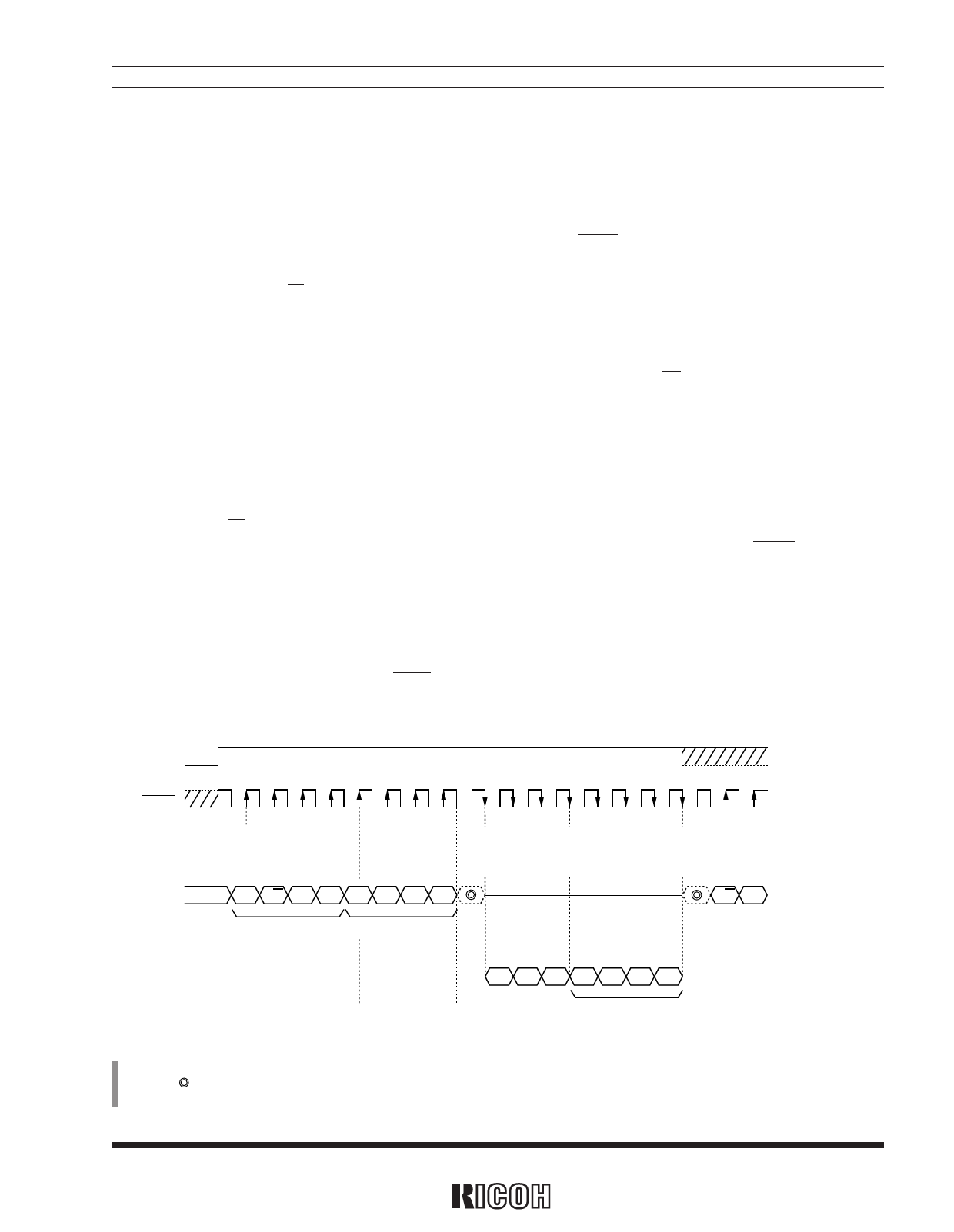
2.1 Read Cycle Flow
1. The CE pin is switched from the low level to the high level.
2. Four control bits (with the first bit ignored) and four read address bits are input from the SIO pin. At this time,
control bits R/W and AD are set equally to 1 while a control bit DT is set to 0.
3. The SIO pin enters the output mode at the falling edge of the shift clock pulse 2B from the SCLK pinwhile the
four read bits (MSB→LSB) at designated addresses are output at the falling edge of the shift clock pulse 5B (see
the figure below).
4. Then, the SIO pin returns to the input mode at the falling edge of the shift clock pulse 1C. Afterwards control bits
and address bits are input at the shift clock pulses 1C in the same manner as at the shift clock pulse 1A.
5. At the end of read cycle, the CE pin is switched from the high level to the low level (after tCEH from the rising edge
of the eighth shift clock pulse from the SCLK pin). (Following on read cycle, write operation can be performed by
setting control bits in the write mode at the shift clock pulse 1C and later with the CE pin held at the high level.)
CE
SCLK
1A 2A 3A 4A 5A 6A 7A 8A 1B 2B 3B 4B 5B 6B 7B 8B 1C 2C 3C
Input to
SIO pin
Reading to shift register
*
* R/W AD DT A3 A2 A1 A0
Control bits
Address bits
Setting of Shifting data
SIO pin in
output mode
(Hi-z)
Setting of SIO pin in
input mode
R/W AD
Output from
SIO pin
(Hi-z)
(Internal processing)
Setting of
control bit
— — — D3 D2 D1 D0
Writing to
address resister
Read data
(Hi-z)
* * ) In the above figure, the “ ” mark indicates arbitrary data; the “—” mark indicates unknown data;
the“ ” mark indicates data which are available when the SIO pin is held at the high, low, or Hiz level ;
and the diagonaliy shaded area indicates high or low.
3
Share Link: 