ML7041 Просмотр технического описания (PDF) - Unspecified
Номер в каталоге
Компоненты Описание
производитель
ML7041 Datasheet PDF : 28 Pages
| |||
FEDL7041-05
ML7041
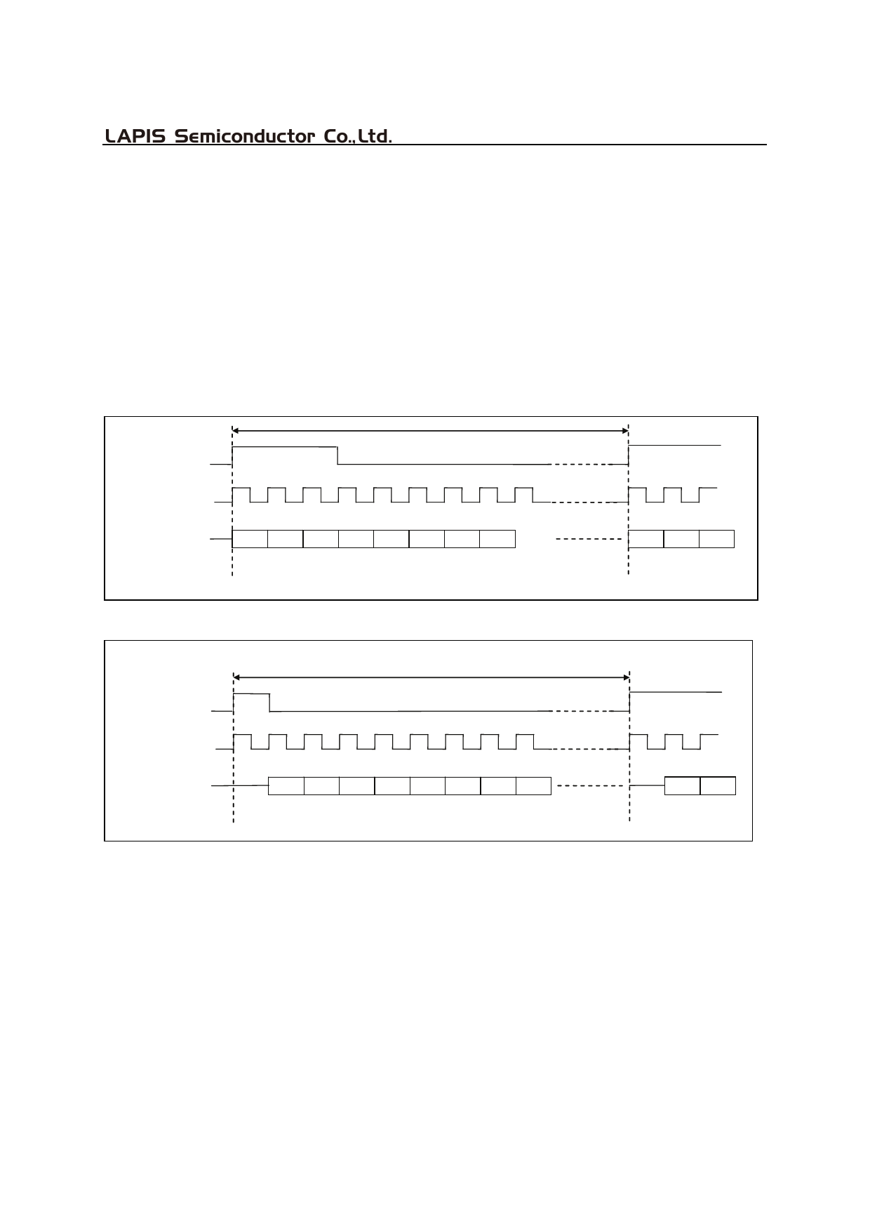
SYNC
8 kHz synchronous signal input for transmit and receive PCM data.
Synchronize this signal with BCLK signal. This signal is used to indicate the MSB of the PCM data stream.
PCMOUT
Transmit PCM data output. The PCM output signal is output from MSB, synchronously with the rising edges of
BCLK and SYNC. Refer to Figure 2. This is a logic output pin so that external pull-up is not required. This pin
outputs logic "L" except during effective PCM data bits, and outputs logic "H" during power-down.
PCMIN
Receive PCM data input.
The PCM input signal is shifted in on the falling edge of BCLK and is input from MSB.
SYNC
BCLK
PCMIN or
PCMOUT
MSB
Refer to Figure 2.
8 kHz (125 µs)
LSB
* 14 bits when linear mode is selected
(a) Long frame synchronous interface
SYNC
BCLK
PCMIN or
PCMOUT
8 kHz (125 µs)
MSB
LSB
* 14 bits when linear mode is selected
(b) Short frame synchronous interface
Figure 2 PCM Interface Basic Timing Diagram
8/28
Share Link: 