ML7041 Просмотр технического описания (PDF) - Unspecified
Номер в каталоге
Компоненты Описание
производитель
ML7041 Datasheet PDF : 28 Pages
| |||
FEDL7041-05
ML7041
FUNCTIONAL DESCRIPTION
Control Registers
CR0 (Basic operating mode 1)
Note: The initial value means a value set when the device is reset by the PDN pin.
CR0
Initial value
B7
B6
B5
B4
B3
B2
B1
B0
A/ SPOUT PDN
SEL
PON
ALL
PDN
TX
PDN
RX
SLP
SLP
SEL
LNR
0
0
0
0
0
0
0
0
B7 ....... PCM interface companding law select 0: -law 1: A-law
B6 ....... Power-on control for output amplifies (SPO+, SPO) 0: Power down 1: Power on
B5 ....... Power down (entire circuitry)
0: Power on 1: Power down
ORed with the inverted PDN signal. When using this data, set PDN to “L”.
The control registers are not reset by this signal.
B4 ....... Power down (transmit only)
0: Power on 1: Power down
B3 ....... Power down (receive only)
0: Power on 1: Power down
B2 ....... Slope filter enable
0: Slope filter disable 1: Slope filter enable
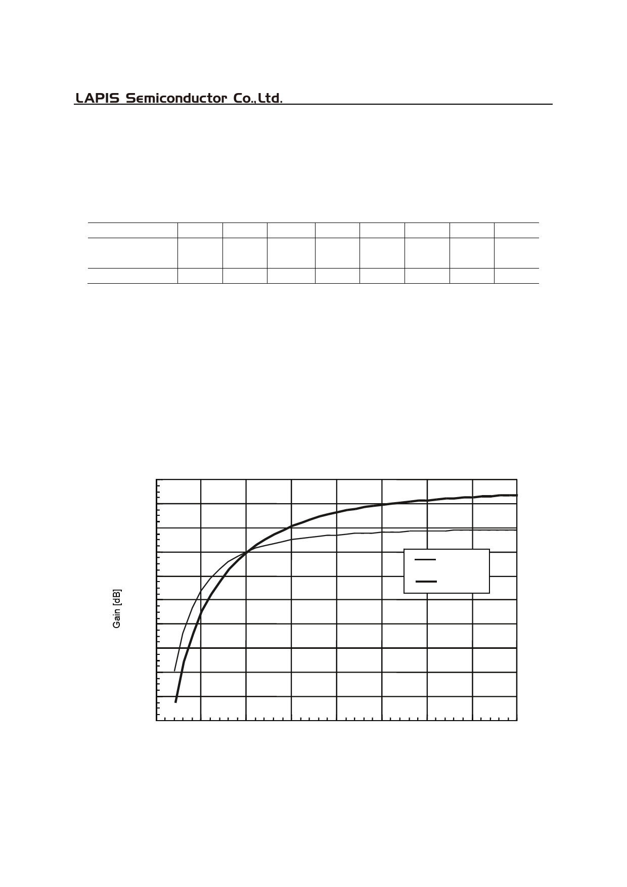
B1 ....... Slope filter frequency response select 0: CASE1 1: CASE2
Either CASE1 or CASE2 can be selected in Figure 8.
B0 ....... PCM interface linear code select
0: PCM companding law selected by CR0-B7
1: 14-bit linear code (2’s complement)
6
4
2
0
–2
–4
–6
–8
–10
–12
–14
0
CASE1
CASE2
500
1000
1500
2000
2500
3000
Frequency [Hz]
Figure 8 Slope Filter Frequency Characteristics
3500
4000
19/28
Share Link: 