MTW14N50E Просмотр технического описания (PDF) - ON Semiconductor
Номер в каталоге
Компоненты Описание
производитель
MTW14N50E Datasheet PDF : 8 Pages
| |||
MTW14N50E
POWER MOSFET SWITCHING
Switching behavior is most easily modeled and predicted
by recognizing that the power MOSFET is charge
controlled. The lengths of various switching intervals (∆t)
are determined by how fast the FET input capacitance can
be charged by current from the generator.
The published capacitance data is difficult to use for
calculating rise and fall because drain–gate capacitance
varies greatly with applied voltage. Accordingly, gate
charge data is used. In most cases, a satisfactory estimate of
average input current (IG(AV)) can be made from a
rudimentary analysis of the drive circuit so that
t = Q/IG(AV)
During the rise and fall time interval when switching a
resistive load, VGS remains virtually constant at a level
known as the plateau voltage, VSGP. Therefore, rise and fall
times may be approximated by the following:
tr = Q2 x RG/(VGG – VGSP)
tf = Q2 x RG/VGSP
where
VGG = the gate drive voltage, which varies from zero to VGG
RG = the gate drive resistance
and Q2 and VGSP are read from the gate charge curve.
During the turn–on and turn–off delay times, gate current is
not constant. The simplest calculation uses appropriate
values from the capacitance curves in a standard equation for
voltage change in an RC network. The equations are:
td(on) = RG Ciss In [VGG/(VGG – VGSP)]
td(off) = RG Ciss In (VGG/VGSP)
The capacitance (Ciss) is read from the capacitance curve at
a voltage corresponding to the off–state condition when
calculating td(on) and is read at a voltage corresponding to the
on–state when calculating td(off).
At high switching speeds, parasitic circuit elements
complicate the analysis. The inductance of the MOSFET
source lead, inside the package and in the circuit wiring
which is common to both the drain and gate current paths,
produces a voltage at the source which reduces the gate drive
current. The voltage is determined by Ldi/dt, but since di/dt
is a function of drain current, the mathematical solution is
complex. The MOSFET output capacitance also
complicates the mathematics. And finally, MOSFETs have
finite internal gate resistance which effectively adds to the
resistance of the driving source, but the internal resistance
is difficult to measure and, consequently, is not specified.
The resistive switching time variation versus gate
resistance (Figure 10) shows how typical switching
performance is affected by the parasitic circuit elements. If
the parasitics were not present, the slope of the curves would
maintain a value of unity regardless of the switching speed.
The circuit used to obtain the data is constructed to minimize
common inductance in the drain and gate circuit loops and
is believed readily achievable with board mounted
components. Most power electronic loads are inductive; the
data in the figure is taken with a resistive load, which
approximates an optimally snubbed inductive load. Power
MOSFETs may be safely operated into an inductive load;
however, snubbing reduces switching losses.
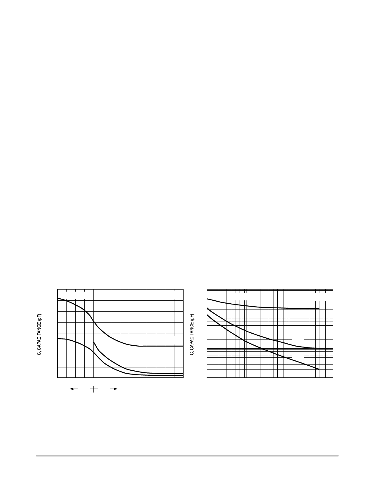
8000
VDS = 0 V
7000
6000
VGS = 0 V
TJ = 25°C
5000
4000
Ciss
3000
2000
Coss
1000
0
10
5
Crss
0
5
10
15
20
25
VGS VDS
GATE-TO-SOURCE OR DRAIN-TO-SOURCE VOLTAGE (VOLTS)
Figure 7a. Low Voltage Capacitance Variation
10000
2000
1000
TJ = 25°C
VGS = 0 V
Ciss
200
Coss
100
Crss
20
10
12
10 20
100 200
1000
VDS, DRAIN-TO-SOURCE VOLTAGE (VOLTS)
Figure 7b. High Voltage Capacitance Variation
http://onsemi.com
4
Share Link: 