BCR10CS-12LB-T11 –Я—А–Њ—Б–Љ–Њ—В—А —В–µ—Е–љ–Є—З–µ—Б–Ї–Њ–≥–Њ –Њ–њ–Є—Б–∞–љ–Є—П (PDF) - Renesas Electronics
–Э–Њ–Љ–µ—А –≤ –Ї–∞—В–∞–ї–Њ–≥–µ
–Ъ–Њ–Љ–њ–Њ–љ–µ–љ—В—Л –Ю–њ–Є—Б–∞–љ–Є–µ
–њ—А–Њ–Є–Ј–≤–Њ–і–Є—В–µ–ї—М
BCR10CS-12LB-T11
Renesas Electronics

BCR10CS-12LB-T11 Datasheet PDF : 8 Pages
| |||
BCR10CS-12LB (The product guaranteed maximum junction temperature of 150°C)
Parameter
RMS on-state current
Surge on-state current
I2t for fusing
Peak gate power dissipation
Average gate power dissipation
Peak gate voltage
Peak gate current
Junction temperature
Storage temperature
Mass
Notes: 1. Gate open.
Symbol
IT (RMS)
ITSM
I2t
PGM
PG (AV)
VGM
IGM
Tj
Tstg
вАФ
Ratings
10
100
41.6
5
0.5
10
2
вАУ 40 to +150
вАУ 40 to +150
1.2
Unit
Conditions
A
Commercial frequency, sine full wave
360° conduction, Tc = 128°CNote3
A
60Hz sinewave 1 full cycle, peak value,
non-repetitive
A2s
Value corresponding to 1 cycle of half
wave 60Hz, surge on-state current
W
W
V
A
°C
°C
g
Typical value
Electrical Characteristics
Parameter
Symbol Min. Typ. Max. Unit
Test conditions
Repetitive peak off-state current
IDRM
вАФ
On-state voltage
VTM
вАФ
Gate trigger voltageNote2
ќЩ
VFGTќЩ
вАФ
ќЩќЩ
VRGTќЩ
вАФ
ќЩќЩќЩ
VRGTќЩќЩќЩ
вАФ
Gate trigger currentNote2
ќЩ
IFGTќЩ
вАФ
ќЩќЩ
IRGTќЩ
вАФ
ќЩќЩќЩ
IRGTќЩќЩќЩ
вАФ
вАФ
2.0
mA Tj = 150°C, VDRM applied
вАФ
1.5
V Tc = 25°C, ITM = 15 A,
Instantaneous measurement
вАФ
1.5
V Tj = 25¬∞C, VD = 6 V, RL = 6 вД¶,
вАФ
1.5
V
RG = 330 вД¶
вАФ
1.5
V
вАФ
30Note6 mA Tj = 25¬∞C, VD = 6 V, RL = 6 вД¶,
вАФ
30Note6
mA
RG = 330 вД¶
вАФ
30Note6
mA
Gate non-trigger voltage
Thermal resistance
Critical-rate of rise of off-state
commutating voltageNote5
VGD
0.2/0.1
вАФ
Rth (j-c)
вАФ
вАФ
(dv/dt)c 10/1
вАФ
вАФ
V
Tj = 125°C/150°C, VD = 1/2 VDRM
1.8
°C/W Junction to caseNote3 Note4
вАФ
V/µs Tj = 125°C/150°C
Notes: 2. Measurement using the gate trigger characteristics measurement circuit.
3. Case temperature is measured on the T2 tab.
4. The contact thermal resistance Rth (c-f) in case of greasing is 1.0°C/W.
5. Test conditions of the critical-rate of rise of off-state commutating voltage is shown in the table below.
6. High sensitivity (IGT вЙ§ 20 mA) is also available. (IGT item: 1)
Test conditions
1. Junction temperature
Tj = 125°C/150°C
2. Rate of decay of on-state commutating current
(di/dt)c = вАУ 5.0 A/ms
3. Peak off-state voltage
VD = 400 V
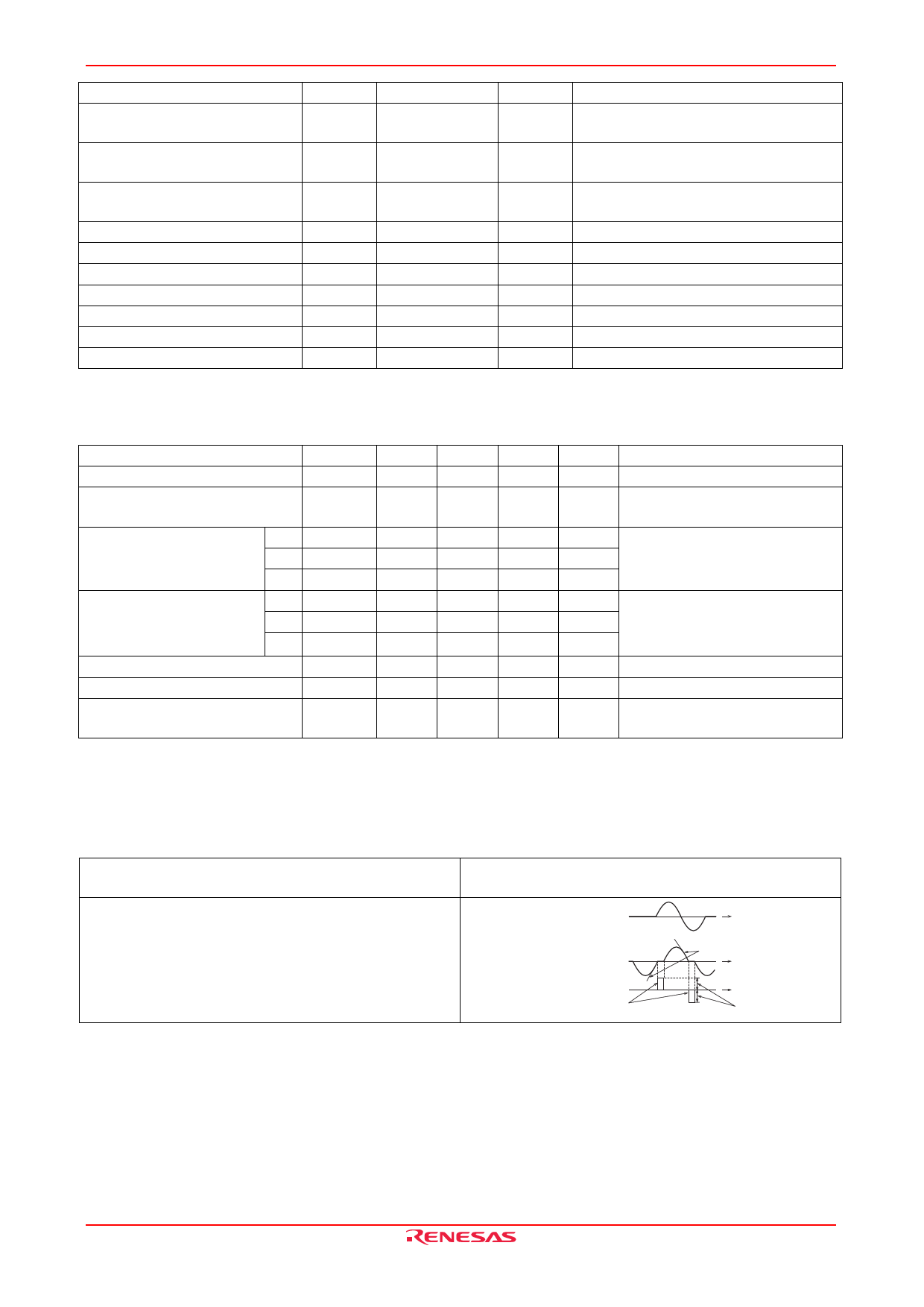
Commutating voltage and current waveforms
(inductive load)
Supply Voltage
Time
Main Current
Main Voltage
(dv/dt)c
(di/dt)c
Time
Time
VD
REJ03G0469-0300 Rev.3.00 Nov 30, 2007
Page 2 of 7
Share Link: