STR-F6600 Просмотр технического описания (PDF) - Allegro MicroSystems
Номер в каталоге
Компоненты Описание
производитель
STR-F6600 Datasheet PDF : 16 Pages
| |||
Series STR-F6600
OFF-LINE
QUASI-RESONANT FLYBACK
SWITCHING REGULATORS
Functional Description and Operation (cont’d)
The drive winding voltage is set such that in normal
operation the C2 voltage is above the specified maximum
shutdown voltage (11 V) and below the specified mini-
mum over-voltage threshold (20.5 V).
In applications where there is a significant variation in
load current, the VIN terminal voltage may vary, as shown
in figure 4. This is due to peak charging of C2. In this
case, adding a resistor in the range of a few ohms to tens of
ohms in series with the rectifier diode D2 will bring the
voltage variation within limits.
VIN
comparator output pre-terminates the oscillator, which
turns off the MOSFET drive signal.
The MOSFET is turned on again when either cSS
discharges or a quasi-resonance signal is detected on pin 1.
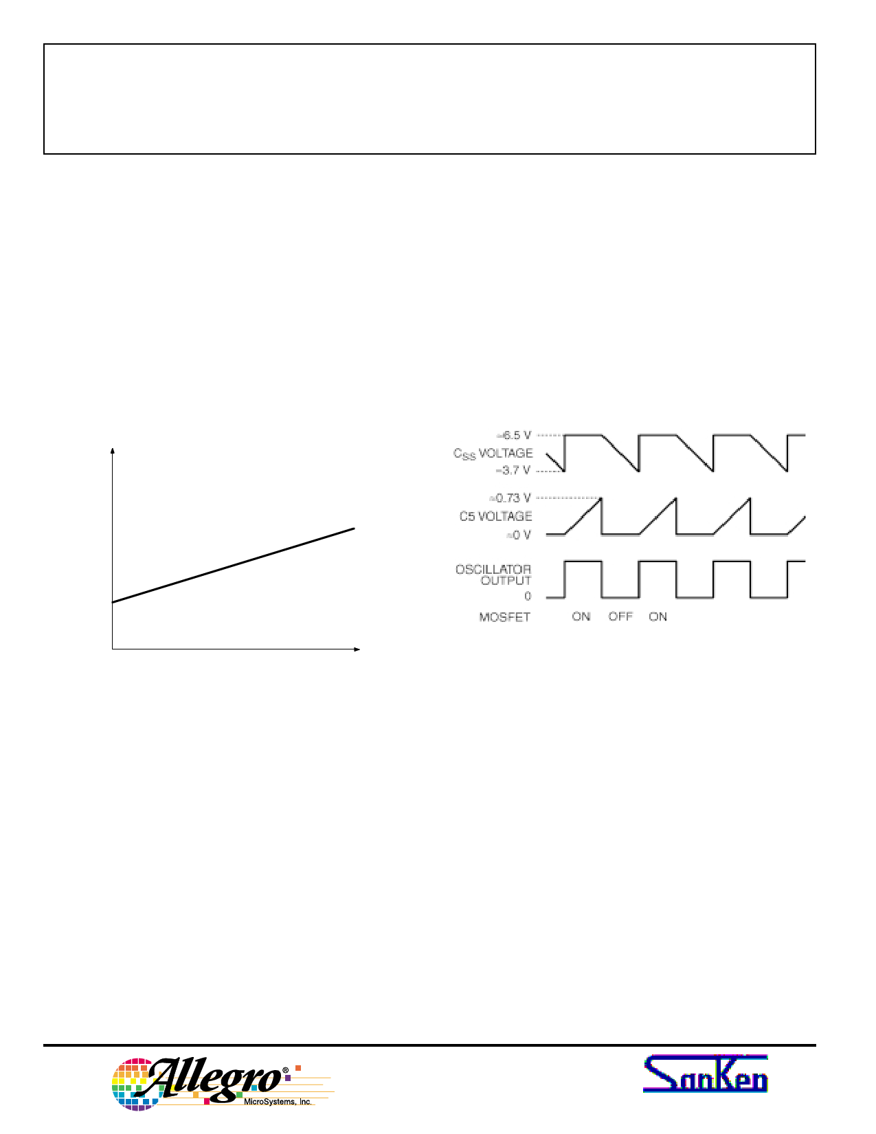
Fixed 50 µs Off-Time: Soft-Start Mode
This is the mode of operation in the absence of a quasi-
resonance signal on pin 1 (see figure 5), and occurs at
IOUT
Figure 4 – Output Current IOUT – Terminal Voltage VIN
Soft Start, Quasi Resonant and Voltage Regulation
Refer to the Functional Block Diagram and the Typical
Application Diagram (figure 6). The internal oscillator
uses the charge/discharge of an internal 4700 pF capacitor
(cSS) to generate the MOSFET drive signals.
The regulator has two modes of operation:
1. fixed 50 µs off time (soft start) and
2. demagnetization sensing quasi-resonant mode —
normal operation.
In both cases, voltage regulation is achieved by taking
the composite optocoupled voltage error and superimposed
drain current ramp (current-mode control) and comparing
this to an internal 0.73 V reference. The FBK/OCP
Figure 5 – Soft-Start Operation
startup and in overload. It also can be commanded exter-
nally to provide low-power standby operation.
In the absence of a feedback signal (such as at startup,
or a short circuit) the drain current ramp, sensed across R5
and noise filtered by R4/C5 appears on pin 1. When the
ramp voltage on C5 exceeds the 0.73 V reference signal,
the FBK/OCP comparator changes state, shutting down the
oscillator and turning off the MOSFET. Thus the voltage
on cSS is held high (6.5 V) by the comparator. When the
comparator changes state, cSS discharges via rSS; the
voltage on cSS ramps down until it reaches 3.7 V. The
oscillator turns on the MOSFET. This ramp-down time is
internally trimmed to 50 µs. The comparator changes state
again and the cycle repeats. Thus in the absence of
feedback, the current-sense resistor R5 accurately controls
the MOSFET maximum current.
™TM
6
115 Northeast Cutoff, Box 15036
Worcester, Massachusetts 01615-0036 (508) 853-5000
Share Link: 