UPD720130 Просмотр технического описания (PDF) - NEC => Renesas Technology
Номер в каталоге
Компоненты Описание
производитель
UPD720130 Datasheet PDF : 44 Pages
| |||
µPD720130
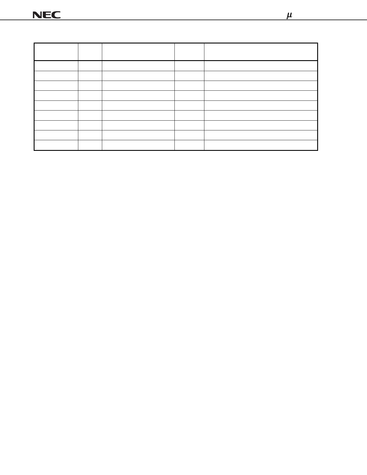
Pin Name
I/O
Buffer Type
Active
Level
Function
(2/2)
GPIO(7:0)
I/O 3.3 V Schmitt I/O
General purpose IO port (for future extension)
PIO(15:14)
I/O 3.3 V I/O
IO port (for future extension)
PIO(5)
I/O 3.3 V Schmitt I/O
IO port (for future extension)
IRQ0
I
3.3 V Schmitt Input
High
External interrupt input (for future extension)
AVDD25
2.5 V VDD for Analog circuit
VDD25
2.5 V VDD
VDD33
3.3 V VDD
AVSS
VSS for Analog circuit
VSS
VSS
Remarks 1. “5 V tolerant“ means that the buffer is 3.3 V buffer with 5 V tolerant circuit.
2. The signal marked as “(I/O)” in the above table operates as I/O signals during testing. However, they
do not need to be considered in normal use.
6
Data Sheet S16302EJ3V0DS
Share Link: 