MX165C Просмотр технического описания (PDF) - MX-COM Inc
Номер в каталоге
Компоненты Описание
производитель
MX165C Datasheet PDF : 15 Pages
| |||
Low Voltage CTCSS Encoder/Decoder
4
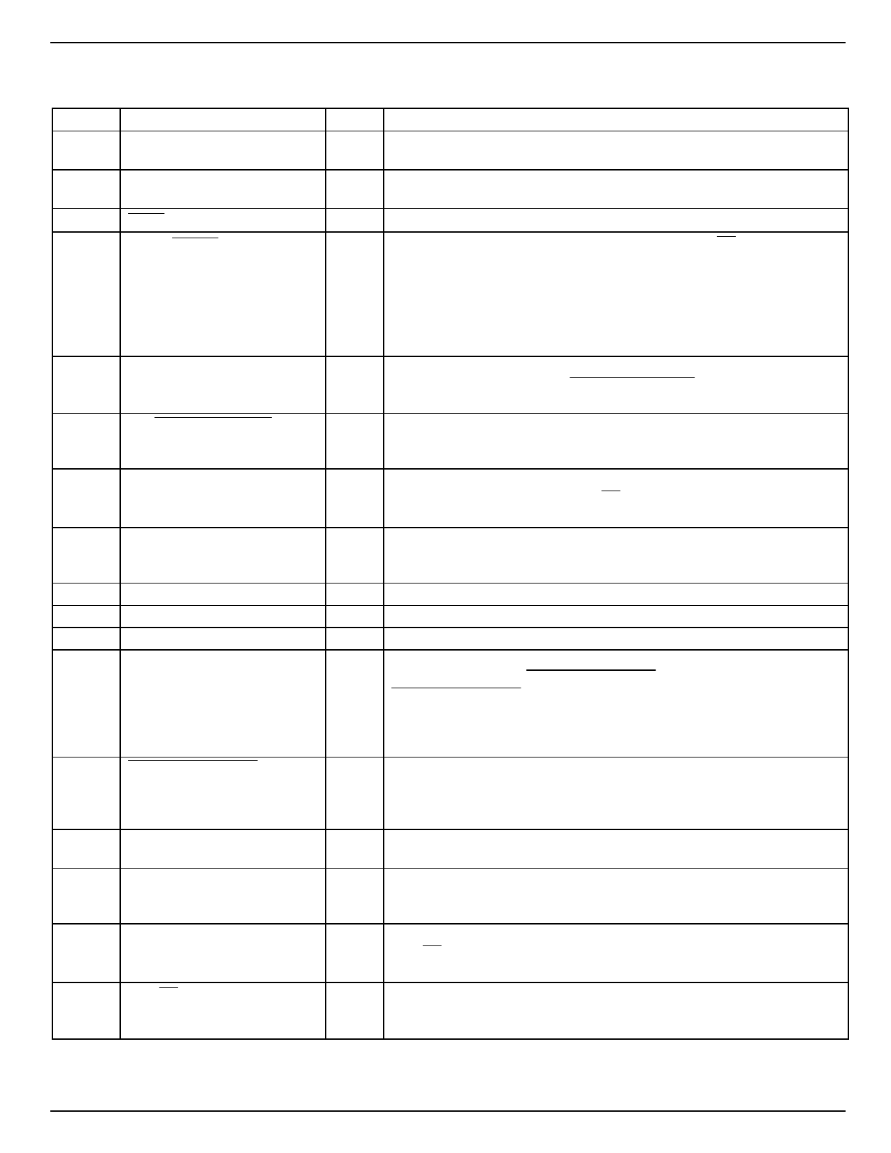
Signal List
MX165C
Pin No.
1
VDD
Signal
2 XTAL/CLOCK
3
XTAL
4
LOAD/LATCH
5 D5 / SERIAL ENABLE 1
6 D4 / SERIAL ENABLE 2
7 D3 / SERIAL DATA IN
8 D2 / SERIAL CLOCK
9 D1
10 D0
11 VSS
12 DECODE COMPARATOR
REF.
13 RX TONE DECODE
14 DECODE COMPARATOR IN
15 RX TONE DETECT
16 TX TONE OUT
17 RX / TX
Type
Description
power Positive supply. This pin should be bypassed to VSS by a capacitor
mounted close to the device pins.
input Input to the on-chip inverter used with a 1MHz Xtal or external clock
source.
output Output of the on-chip inverter (clock output).
input
input
input
input
input
input
input
power
Controls 8 on-chip latches. It is used to latch RX / TX , PTL, and D0-
D5. A logic 1 applied to this input places the 8 latches in the
‘transparent’ mode. A logic 0 applied to this input places the 8 latches
in the ‘latched’ mode. In Parallel Mode, data is loaded and latched by
a logic 1-0 transition (see Figure 4). In Serial Mode, data is loaded
and latched by a 0-1-0 strobe pulse on this pin (see Figure 5).
Internally pulled to VDD
Data input D5 (Parallel Mode). A logic 1 applied to this input together
with a logic 0 applied to D4/SERIAL ENABLE 2 will place the device
in Serial Mode (see Figure 5). Internally pulled to VDD.
Data input D4 (Parallel Mode). A logic 0 applied to this input together
with a logic 1 applied to D5 / SERIAL ENABLE 1 will place the device
in Serial Mode (see Figure 5). Internally pulled to VDD.
Data input D3 (Parallel Mode). In Serial Mode this pin becomes the
serial data input for D5-D0, RX / TX and PTL (see Figure 5). D5 is
clocked first and PTL last. Internally pulled to VDD.
Data input D2 (Parallel Mode). In Serial Mode this pin becomes the
SERIAL CLOCK input. Data is clocked on the positive going edge
(see Figure 5). Internally pulled to VDD.
Data input D1 (Parallel Mode). Internally pulled to VDD.
Data input D0 (Parallel Mode). Internally pulled to VDD.
Negative supply.
input
Internally biased to VDD/3 or 2 VDD/3 via 1M resistors depending on
the logic state of the RX TONE DECODE pin.
RX TONE DECODE = 1 will bias this input 2 VDD/3; a logic 0 will bias
this input VDD/3. This input provides the DECODE COMPARATOR
REFERENCE voltage, and the switching of bias voltages provides
hysteresis to reduce ‘chatter’ under marginal conditions.
output
Gated output of the decode comparator. This output is used to gate
the RX Audio path. A logic 0 on this pin indicates a successful
decode and the DECODE COMPARATOR IN pin is more positive
than the DECODE COMPARATOR REF. input (see Table 3).
input Inverting input of the DECODE COMPARATOR. This pin is normally
connected to the integrated output of the RX TONE DETECT line.
output In RX mode this output will go to logic 1 during a successful decode.
It must be externally integrated to control response and deresponse
times (see Table 3).
output
input
The CTCSS sinewave output appears on this pin under control of the
RX / TX pin. When not transmitting a tone, TX TONE OUT may be
biased to VDD/2. (see Table 3).
RX or TX modes selected in Parallel Mode (see Figure 4). In Serial
Mode this function is serially loaded. This pin is internally pulled to
VDD via a 1MΩ resistor.
© 1997 MX•COM Inc.
www.mxcom.com Tele: 800 638-5577 910 744-5050 Fax: 910 744-5054
Doc. # 20480102.008
4800 Bethania Station Road, Winston-Salem, NC 27105-1201 USA All trademarks and service marks are held by their respective companies.
Share Link: 