MT6305B Просмотр технического описания (PDF) - MediaTek Inc
Номер в каталоге
Компоненты Описание
производитель
MT6305B Datasheet PDF : 34 Pages
| |||
Confidential Information
MT6305B
Absolute Maximum Ratings
CHRIN and GATEDRV relative to GND....-0.3V to 15V
LED, ALERTER, VIBRATOR and VREF relative to
GND… … … … … … … … … ..… ..… … -0.3V to Vbat+0.3V
All other pins relative to GND… … … … .… … -0.3V to 7V
Operating Temperature Ranges..… ...… -25°C to +85°C
Maximum Junction Temperature .… … ..… .… … +165°C
Storage Temperature Range.… ...… ..… -65°C to +165°C
Thermal Impedance, θJA(4 layer JEDEC PCB)....23°C/W
Reflow Temperature (soldering, 10sec).… ........+260°C
Stresses beyond those listed under ”Absolute Maximum Ratings” may cause permanent damage to the device. These are stress rat-
ings only, and functional operation of the device at these or any other conditions beyond those indicated in the operational sections of
specifications is not implied. Exposure to absolute maximum rating conditions for extended periods may affect device reliability.
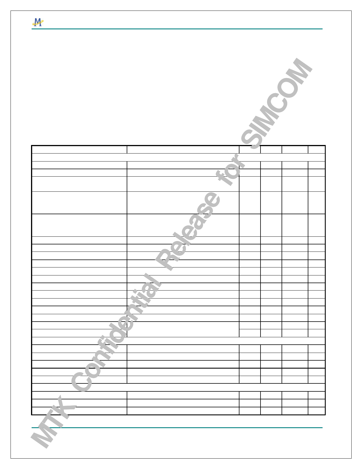
Electrical Characteristics
(Vbat=3V -5.5V, CVa=4.7µF, CVrtc=0.22µF, CVcore=CVm=CVref=CVtcxo=CVsim=CVio=2.2µF, minimum
loads applied on all outputs, unless otherwise noted. Typical values are at TA=+25°C.)
PARAMETER
CONDITION
MIN
Main Controller
Battery Input Voltage Range
3
Charger Input Voltage Range
---
Valid_CHRIN maximum CHRIN voltage Charger will terminate charging automatically-
8.0
when CHRIN is above the voltage
Shutdown Supply Cu rrent
Vbat<2.5V
---
2.5V<Vbat<3.2V
3.2V<Vbat
Operation Ground Cu rrent
All Output on
---
Vtcxo off, all others on
Va, Vtcxo off, all others on
UVLO on Threshold
Vbat; Falling edge
2.85
UVLO Hysteresis
Vbat
250
Deep Discharging Lockout on Threshold Vbat Falling edge
2.35
Deep Discharging Lockout Hysteresis Vbat
100
Thermal Shutdown Threshold
---
Thermal Shutdown Hysteresis
---
LDO Enable Response Time
---
Power Key Input High Voltage
PWRKEY
0.7xVbat
Power Key Input Low Voltage
PWRKEY
---
PWRBB Input High Voltage
PWRBB
1
PWRBB Input Low Voltage
PWRBB
---
Control Input High Voltage
VMSEL, SIMSEL, SIMVCC, SRCLKEN, VASEL, 2
Control Input Low Voltage
BATUSE, LEDEN, VIBRATOREN, ALERTEREN ---
Digital Core Voltage LDO (Vcore)
1.8V Output Voltage
1.7
1.2V Output Voltage
1.1
Output Short Current Limit
---
Load Regulation
0.05mA <I_load< 200mA
---
Line Regulation
3.6V <Vbat< 5.5V
---
Digital IO Voltage LDO (Vio)
Output Voltage
2.7
Output Short Current Limit
---
Load Regulation
0.05mA<I_load<100mA at Vbat=3.6V
---
TYP
---
---
9.0
20
45
45
187
148
108
2.9
300
2.5
200
165
40
250
---
---
---
---
---
---
1.8
1.2
430
1.3
3.3
2.8
275
3
MAX UNIT
5.5
V
15
V
9.5
V
40
75
µA
80
500
200
µA
150
2.95
V
350
mV
2.65
V
300
mV
---
°C
---
°C
---
µs
---
V
0.3x Vbat V
---
0.2
---
V
0.8
V
1.9
V
1.3
V
---
mA
20
mV
6
mV
2.9
V
---
mA
10
mV
MediaTek Confidential
Revision 1.1–Apr. 22, 2005
© 2002 MediaTek Inc.
The information contained in this document can be modified without notice
Page 9 of 33
Share Link: 