CAT1163 Просмотр технического описания (PDF) - ON Semiconductor
Номер в каталоге
Компоненты Описание
производитель
CAT1163 Datasheet PDF : 12 Pages
| |||
CAT1163
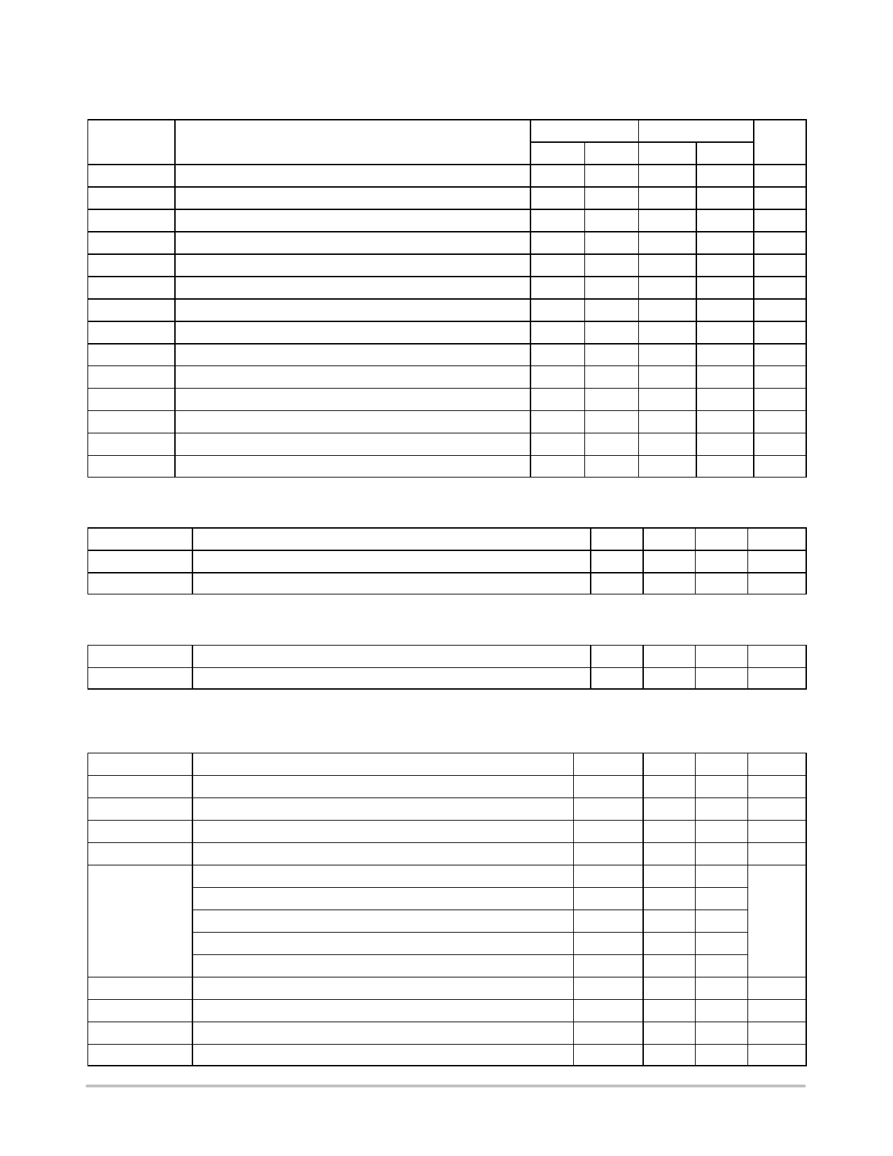
Table 6. AC CHARACTERISTICS
VCC = 2.7 V to 6.0 V unless otherwise specified. Output Load is TTL Gate and 100 pF.
VCC = 2.7 V − 6 V
Symbol
Parameter
Min
Max
FSCL
Clock Frequency
100
T1 (Note 1) Noise Suppression Time Constant at SCL, SDA Inputs
200
tAA
SCL Low to SDA Data Out and ACK Out
3.5
tBUF (Note 1) Time the Bus must be Free Before a New Transmission Can Start
4.7
tHD; STA
Start Condition Hold Time
4
tLOW
Clock Low Period
4.7
tHIGH
Clock High Period
4
tSU; STA
Start Condition Setup Time (for a Repeated Start Condition)
4.7
tHD; DAT
Data in Hold Time
0
tSU; DAT
Data in Setup Time
50
tR (Note 1) SDA and SCL Rise Time
1
tF (Note 1) SDA and SCL Fall Time
300
tSU; STO
Stop Condition Setup Time
4
tDH
Data Out Hold Time
100
1. This parameter is tested initially and after a design or process change that affects the parameter.
VCC = 4.5 V − 5.5 V
Min
Max
400
200
1
1.2
0.6
1.2
0.6
0.6
0
50
0.3
300
0.6
100
Units
kHz
ns
ms
ms
ms
ms
ms
ms
ns
ns
ms
ns
ms
ns
Table 7. POWER−UP TIMING (Notes 1 and 2)
Symbol
Parameter
Min
Typ
tPUR
Power−up to Read Operation
tPUW
Power−up to Write Operation
2. tPUR and tPUW are the delays required from the time VCC is stable until the specific operation can be initiated.
Max Units
1
ms
1
ms
Table 8. WRITE CYCLE LIMITS
Symbol
Parameter
Min
Typ
Max Units
tWR
Write Cycle Time
10
ms
The write cycle time is the time from a valid stop condition of a write sequence to the end of the internal program/erase cycle. During the write
cycle, the bus interface circuits are disabled, SDA is allowed to remain high, and the device does not respond to its slave address.
Table 9. RESET CIRCUIT CHARACTERISTICS
Symbol
Parameter
tGLITCH
VRT
VOLRS
VOHRS
VTH
tPURST
tWP
tRPD
VRVALID
Glitch Reject Pulse Width
Reset Threshold Hysteresis
Reset Output Low Voltage (IOLRS = 1 mA)
Reset Output High Voltage
Reset Threshold (VCC = 5 V), (CAT1163−45)
Reset Threshold (VCC = 5 V), (CAT1163−42)
Reset Threshold (VCC = 3.3 V), (CAT1163−30)
Reset Threshold (VCC = 3.3 V), (CAT1163−28)
Reset Threshold (VCC = 3 V), (CAT1163−25)
Power−Up Reset Timeout
Watchdog Period
VTH to RESET Output Delay
RESET Output Valid
Min
Typ
15
VCC − 0.75
4.50
4.25
3.00
2.85
2.55
130
1.6
1
Max Units
100
ns
mV
0.4
V
V
4.75
V
4.50
3.15
3.00
2.70
270
ms
s
5
ms
V
http://onsemi.com
4
Share Link: 