ATSAMA5D41A-CU Просмотр технического описания (PDF) - Atmel Corporation
Номер в каталоге
Компоненты Описание
производитель
ATSAMA5D41A-CU Datasheet PDF : 1808 Pages
| |||
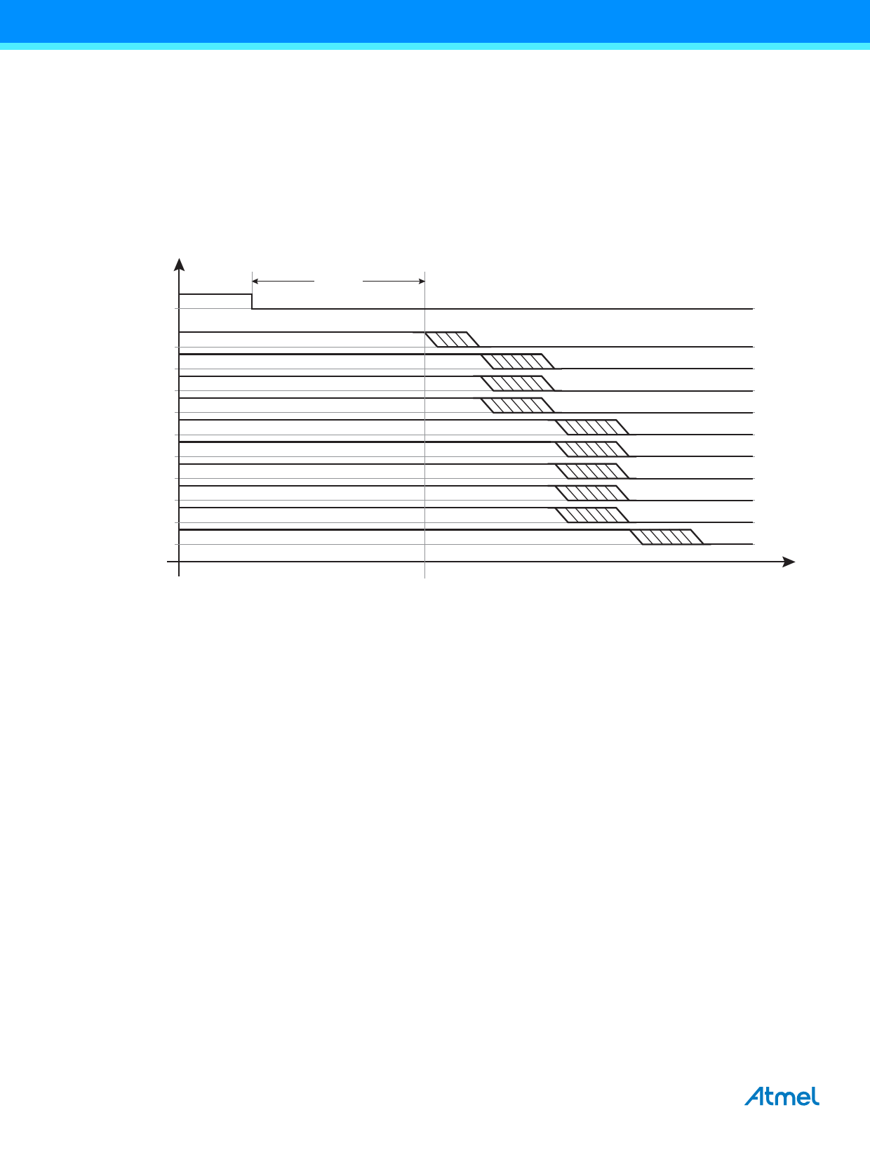
4.5 Powerdown Considerations
The user must maintain NRST at ‘L’ prior to switching off the power supplies. After a delay of five SLCK periods,
the user can switch off VDDCORE, then VDDIOP and VDDANA. Afterward, other power supplies can be switched
off.
VDDBU must never be switched when other supplies are on.
Figure 4-2 illustrates the SAMA5D4 powerdown sequence.
Figure 4-2. Recommended Powerdown Sequence
NRST
VDDCORE
VDDIOP0
VDDIOP1
VDDANA
VDDOSC
VDDIOM
VDDUTMII
VDDIODDR
VDDFUSE
VDDBU
5 x tSLCK
time
4.6 Power-on Reset
The SAMA5D4 embeds several Power-On Resets (POR) to ensure that the power supply is switched on when the
reset is released. These PORs are dedicated to VDDBU, VDDIOP and VDDCORE respectively.
4.7 Programmable I/O Lines and Current Drive
4.7.1
DDR2 Bus interface
16-bit or 32-bit wide interface, supporting:
16-bit or 32-bit DDR2/LPDDR/LPDDR2
The DDR2/LPDDR/LPDDR2 I/Os embeds an automatic impedance matching control to avoid overshoots and to
reach the best performances according to the bus load and external memories.
Two specific analog inputs, DDR_CALP and DDR_CALN are used to calibrate all the DDR I/Os.
4.7.2
LP-DDR2 Power Fail Management
The DDR controller (MPDDRC) allows to manage the LPDDR memory when an uncontrolled power off occurs.
The DDR power rail must be monitored externally and generate an interrupt when a power fail condition is
triggered. The interrupt handler must apply the sequence defined in the MPDDRC Low-power Register by setting
the bit LPDDR2_PWOFF (LPDDR2 Power Off Bit).
30 SAMA5D4 Series [DATASHEET]
Atmel-11238C-ATARM-SAMA5D4-Datasheet_12-Jul-16
Share Link: 