ATSAM3N2BA-MU Просмотр технического описания (PDF) - Atmel Corporation
Номер в каталоге
Компоненты Описание
производитель
ATSAM3N2BA-MU Datasheet PDF : 60 Pages
| |||
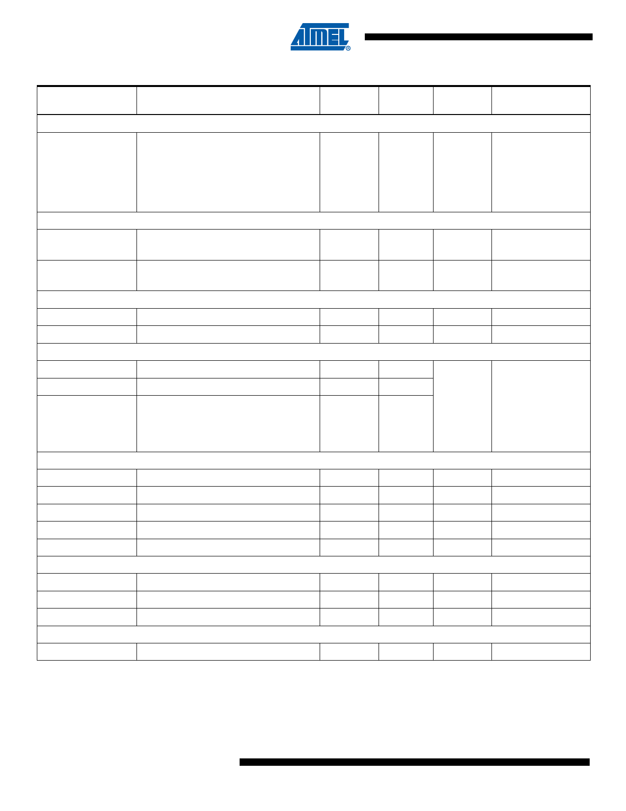
Table 3-1. Signal Description List (Continued)
Signal Name
Function
Type
Flash Memory
Active
Level
Voltage
Reference
ERASE
Flash and NVM Configuration Bits Erase
Command
Input
High
VDDIO
NRST
TST
URXDx
UTXDx
PA0 - PA31
PB0 - PB14
PC0 - PC31
SCKx
TXDx
RXDx
RTSx
CTSx
TCLKx
TIOAx
TIOBx
PWMx
Microcontroller Reset
Reset/Test
I/O
Low
VDDIO
Test Mode Select
Input
VDDIO
Universal Asynchronous Receiver Transceiver - UARTx
UART Receive Data
Input
UART Transmit Data
Output
PIO Controller - PIOA - PIOB - PIOC
Parallel IO Controller A
I/O
Parallel IO Controller B
I/O
Parallel IO Controller C
VDDIO
I/O
Universal Synchronous Asynchronous Receiver Transmitter USARTx
USARTx Serial Clock
I/O
USARTx Transmit Data
I/O
USARTx Receive Data
Input
USARTx Request To Send
Output
USARTx Clear To Send
Input
Timer/Counter - TC
TC Channel x External Clock Input
Input
TC Channel x I/O Line A
I/O
TC Channel x I/O Line B
I/O
Pulse Width Modulation Controller- PWMC
PWM Waveform Output for channel x
Output
Comments
Reset State:
- Erase Input
- Internal pull-down
enabled
- Schmitt Trigger
enabled(1)
Permanent Internal
pull-up
Permanent Internal
pull-down
Reset State:
- PIO or System
IOs(2)
- Internal pull-up
enabled
- Schmitt Trigger
enabled(1)
8 SAM3N Summary
11011BS–ATARM–22-Feb-12
Share Link: 