EN6360QI Просмотр технического описания (PDF) - Enpirion, Inc.
Номер в каталоге
Компоненты Описание
производитель
EN6360QI Datasheet PDF : 24 Pages
| |||
capacitance from 100µF to 1000µF may be placed
beyond the voltage sensing point outside the
control loop. This additional capacitance should
have a minimum ESR of 6mΩ to ensure stable
operation. Most tantalum capacitors will have more
than 6mΩ of ESR and may be used without special
care. Adding distance in layout may help increase
the ESR between the feedback sense point and the
bulk capacitors.
Table 4: Recommended Output Capacitors
Description
47µF, 10V, 20%
X5R, 1206
(2 capacitors needed)
47µF, 6.3V, 20%
X5R, 1206
(2 capacitors needed)
10µF, 6.3V, 10%
X7R, 0805
(Optional 1 capacitor in
parallel with 2x47µF)
MFG
P/N
Taiyo Yuden
LMK316BJ476ML-T
Murata
Taiyo Yuden
Murata
GRM31CR60J476ME19L
JMK316BJ476ML-T
GRM21BR70J106KE76L
Taiyo Yuden
JMK212B7106KG-T
EN6360QI
Table 5: Recommended REXT Resistor
VIN (V)
IMAX (µA)
REXT (kΩ)
2.5 – 4.0
117
15
4.0 – 6.6
88
51
Output ripple voltage is primarily determined by the
aggregate output capacitor impedance. Placing
multiple capacitors in parallel reduces the
impedance and hence will result in lower ripple
voltage.
1 11
1
= + + ...+
Z ZZ
Z
Total
1
2
n
Table 5: Typical Ripple Voltages
Output Capacitor
Configuration
Typical Output Ripple (mVp-p)
2 x 47 µF
<10mV
† 20 MHz bandwidth limit measured on Evaluation Board
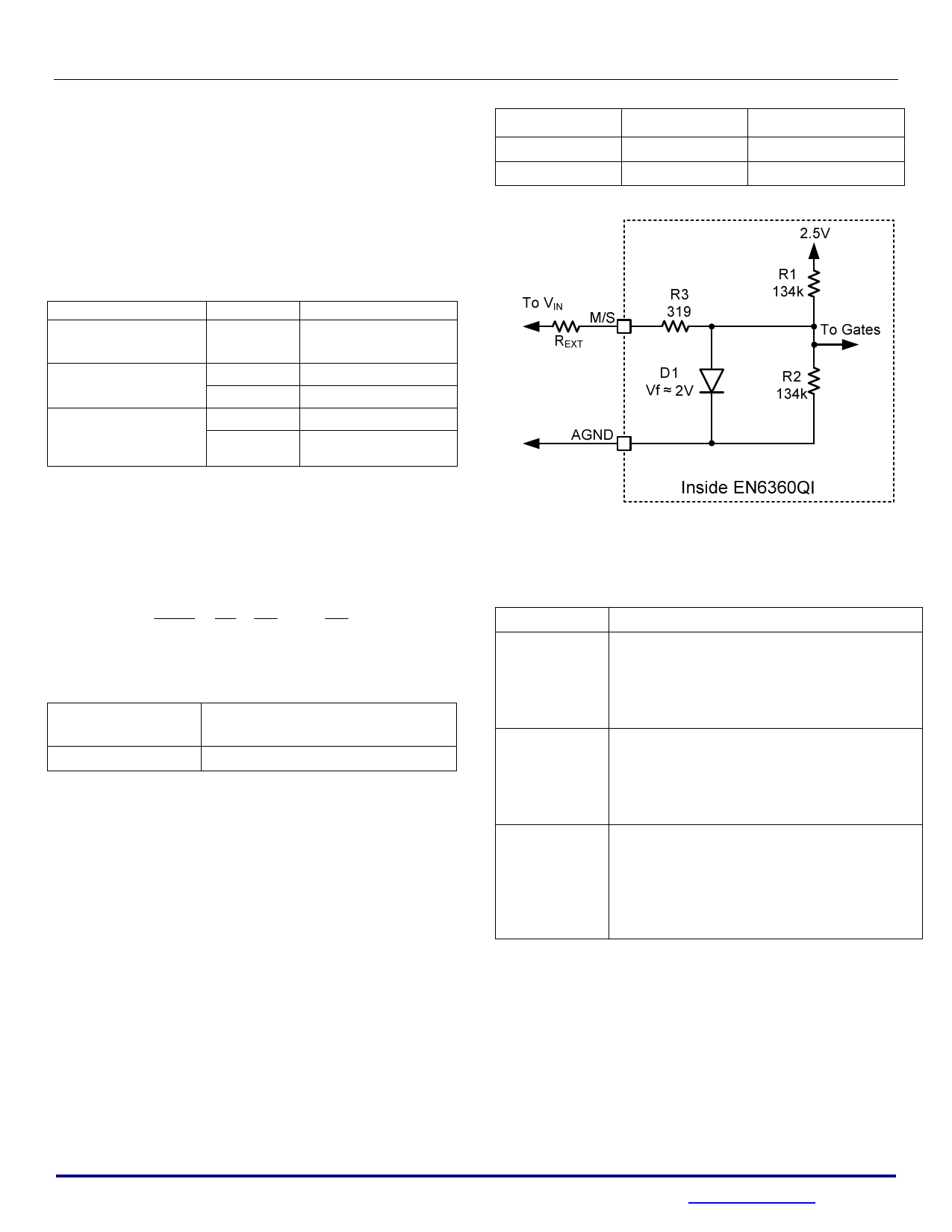
M/S - Ternary Pin
M/S is a ternary pin. This pin can assume 3 states
– A low state (0V to 0.7V), a high state (1.8V to
VIN) and a float state (1.1V to 1.4V). Device
operation is controlled by the state of the pin. The
pins may be pulled to ground or left floating without
any special care. When pulling high to VIN, a series
resistor is recommended. The resistor value may
be optimized to reduce the current drawn by the
pin. The resistance should not be too high as in that
case the pin may not recognize the high state. The
recommend resistance (REXT) value is given in the
following table.
Figure 7: Selection of REXT to Connect M/S pin to VIN
Table 6: M/S (Master/Slave) Pin States
M/S Pin
Low
(0V to 0.7V)
Float
(1.1V to 1.4V)
High
(>1.8V)
Function
M/S pin is pulled to ground directly. This is
the Master mode. Switching PWM phase
will lock onto S_IN external clock if a signal
is available. S_OUT outputs a version of
the internal switching PWM signal.
M/S pin is left floating. Parallel operation is
not feasible. Switching PWM phase will
lock onto S_IN external clock if a signal is
available. S_OUT outputs a version of the
internal switching PWM signal.
M/S pin is pulled to VIN with REXT. This is
the Slave mode. The S_IN signal of the
Slave should connect to the S_OUT of the
Master device. This signal synchronizes
the switching frequency and duty cycle of
the Master to the Slave device.
Power-Up Sequencing
During power-up, ENABLE should not be asserted
before PVIN, and PVIN should not be asserted
before AVIN. Tying all three pins together meets
these requirements.
Technical Suport
Contact Enpirion Applications for additional support
regarding the use of this product
(techsupport@enpirion.com).
©Enpirion 2011 all rights reserved, E&OE
06489
Enpirion Confidential
April 16, 2012
www.enpirion.com, Page 18
Rev: C
Share Link: 