EN6360QI Просмотр технического описания (PDF) - Enpirion, Inc.
Номер в каталоге
Компоненты Описание
производитель
EN6360QI Datasheet PDF : 24 Pages
| |||
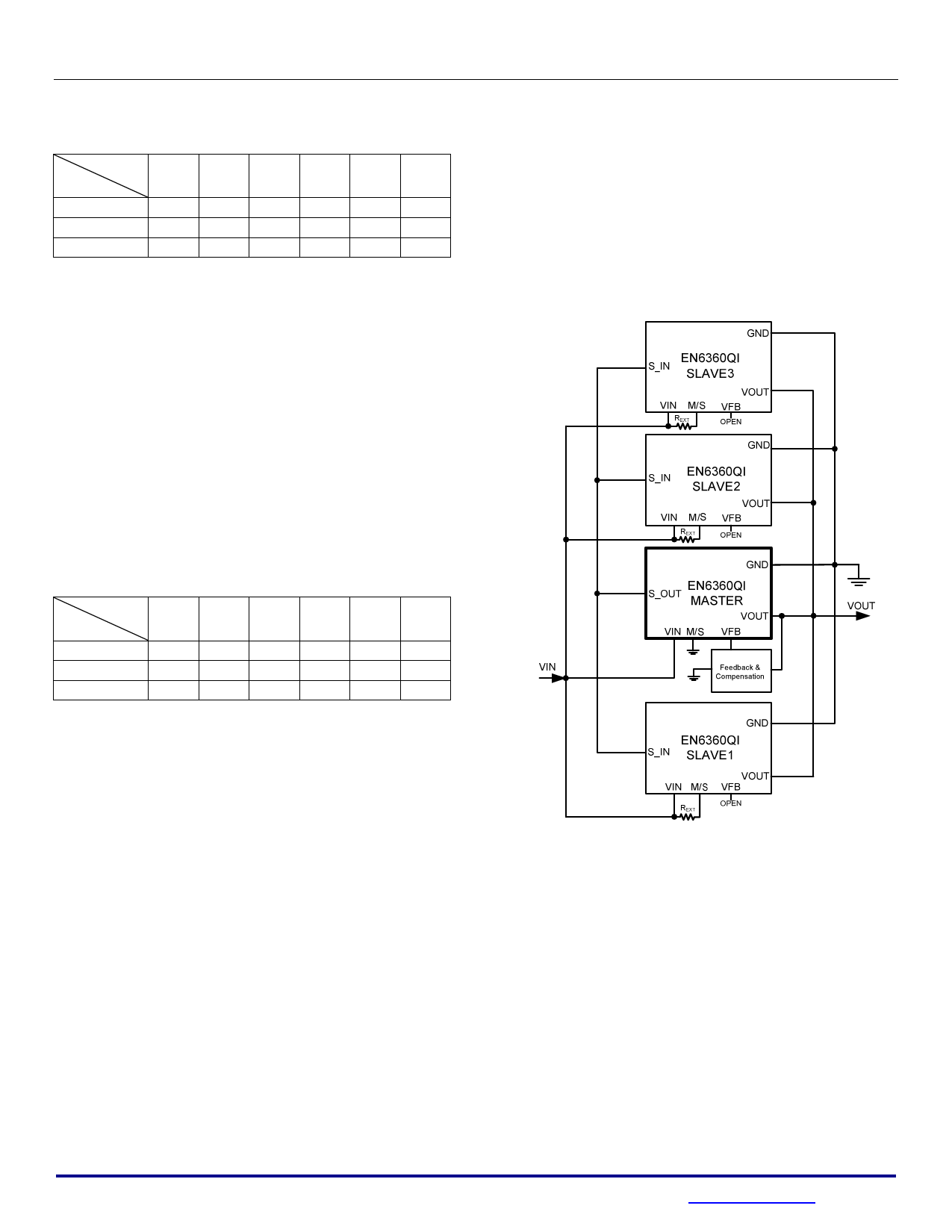
Table 1: Recommended RFQADJ (kΩ)
VOUT
VIN
3.3V ±10%
5.0V ±10%
6.0V ±10%
0.8V
3.57
3.57
3.57
1.2V
3.57
3.57
3.57
1.5V
4.99
4.99
4.99
1.8V
5.49
5.49
5.49
2.5V
5.49
5.49
5.49
3.3V
NA
4.99
5.49
Phase-Lock Operation:
The EN6360QI can be phase-locked to an external
clock signal to synchronize its switching frequency.
The M/S pin can be left floating or pulled to ground
to allow the device to synchronize with an external
clock signal using the S_IN pin. When a clock
signal is present at S_IN, an activity detector
recognizes the presence of the clock signal and the
internal oscillator phase locks to the external clock.
The external clock could be the system clock or the
output of another EN6360QI. The phase locked
clock is then output at S_OUT. Refer to Table 2 for
recommended clock frequencies.
EN6360QI
together with the Master by connecting the S_OUT
of the Master to the S_IN of all other Slave devices.
Refer to Figure 5 for details.
Careful attention is needed in the layout for parallel
operation. The VIN, VOUT and GND of the
paralleled devices should have low impedance
connections between each other. Maximize the
amount of copper used to connect these pins and
use as many vias as possible when using multiple
layers. Place the Master device between all other
Slaves and closest to the point of load.
Table 2: Recommended Clock fsw (MHz)±10%
VOUT
VIN
3.3V ±10%
5.0V ±10%
6.0V ±10%
0.8V
1.15
1.15
1.15
1.2V
1.15
1.15
1.15
1.5V
1.30
1.30
1.30
1.8V
1.35
1.35
1.35
2.5V
1.35
1.35
1.35
3.3V
NA
1.30
1.35
Master / Slave (Parallel) Operation and
Frequency Synchronization
Multiple EN6360QI devices may be connected in a
Master/Slave configuration to handle larger load
currents. The device is placed in Master mode by
pulling the M/S pin low or in Slave mode by pulling
M/S pin high. When the M/S pin is in float state,
parallel operation is not possible. In Master
mode, a version of the internal switching PWM
signal is output on the S_OUT pin. This PWM
signal from the Master is fed to the Slave device at
its S_IN pin. The Slave device acts like an
extension of the power FETs in the Master and
inherits the PWM frequency and duty cycle. The
inductor in the Slave prevents crow-bar currents
from Master to Slave due to timing delays. The
Master device’s switching clock may be phase-
locked to an external clock source or another
EN6360QI to move the entire parallel operation
frequency away from sensitive frequencies. The
feedback network for the Slave device may be left
open. Additional Slave devices may be paralleled
Figure 5: Master/Slave Parallel Operation Diagram
POK Operation
The POK signals that the output voltage is within
the specified range. The POK signal is asserted
high when the rising output voltage crosses 92%
(nominal) of the programmed output voltage. If the
output voltage falls outside the range of 90% to
120%, POK remains asserted for the de-glitch time
(213µs at 1.2MHz). After the de-glitch time, POK is
de-asserted. POK is also de-asserted if the output
voltage exceeds 120% of the programmed output
voltage.
Over Current Protection
The current limit function is achieved by sensing
©Enpirion 2011 all rights reserved, E&OE
06489
Enpirion Confidential
April 16, 2012
www.enpirion.com, Page 15
Rev: C
Share Link: 