USB1T1103 Просмотр технического описания (PDF) - Fairchild Semiconductor
Номер в каталоге
Компоненты Описание
производитель
USB1T1103 Datasheet PDF : 15 Pages
| |||
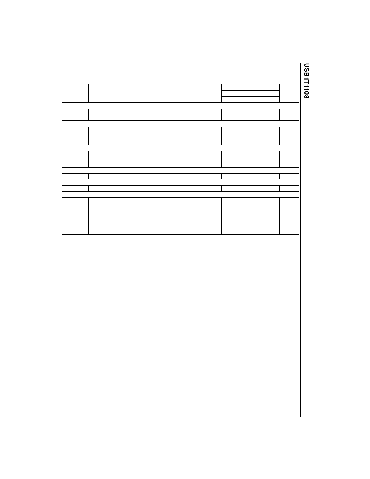
DC Electrical Characteristics (Analog I/O Terminals – D, D Terminals)
Over recommended range of supply voltage and operating free air temperature (unless otherwise noted).
VCC 4.0V to 5.5V or VREG 3.0V to 3.6V
Limits
Symbol
Parameter
Test Condition
40qC to 85qC
Min
Typ
Max
Input Levels – Differential Receiver
VDI
Differential Input Sensitivity
VCM
Differential Common Mode Voltage
INPUT LEVELS – Single-ended Receiver
| VI(D) - VI(D) |
0.2
0.8
2.5
VIL
LOW Level Input Voltage
VIH
HIGH Level Input Voltage
VHYS
Hysteresis Voltage
Output Levels
0.8
2.0
0.30
0.7
VOL
LOW Level Output Voltage
VOH
HIGH Level Output Voltage
RL 1.5k: to 3.6V
RL 15k: to GND
0.3
2.8
3.6
(Note 14)
Leakage Current
IOFF
Input Leakage Current Off State
r1.0
CAPACITANCE
CI/O
Resistance
I/O Capacitance
Terminal to GND
20.0
ZDRV
Driver Output Impedance
34.0
41.0
44.0
(Note 15)
ZIN
RSW
VTERM
Driver Input Impedance
Switch Resistance
Termination Voltage
RPU Upstream Port
10.0
10.0
3.0
3.6
(Note 16)
(Note 17)
Note 14: If VOH min. VREG - 0.2V.
Note 15: Includes external resistors of 27: on both D and D terminals.
Note 16: This voltage is available at terminal VPU and VREG.
Note 17: Minimum voltage is 2.7V in the suspend mode.
Units
V
V
V
V
V
V
V
PA
pF
:
M:
:
V
9
www.fairchildsemi.com
Share Link: 