USB1T1103MHX(2007) Просмотр технического описания (PDF) - Fairchild Semiconductor
Номер в каталоге
Компоненты Описание
производитель
USB1T1103MHX
(Rev.:2007)
(Rev.:2007)
Fairchild Semiconductor

USB1T1103MHX Datasheet PDF : 16 Pages
| |||
Functional Description
The USB1T1103 transceiver is designed to convert
CMOS data into USB differential bus signal levels and to
convert USB differential bus signal to CMOS data.
To minimize EMI and noise the outputs are edge rate
controlled with the rise and fall times controlled and
defined for full speed data rates only (12Mbits/s). The
rise, fall times are balanced between the differential ter-
minals to minimize skew.
The USB1T1103 differs from earlier USB Transceiver in
that the Vp/Vm and Vpo/Vmo terminals are now I/O termi-
nals rather than discrete input and output terminals.
Table 1 describes the specific terminal functionality
selection. Table 2 and Table 3 describe the specific Truth
Tables for Driver and Receiver operating functions.
The USB1T1103 also has the capability of various power
supply configurations, including a disable mode for
VCCIO disconnected, to support mixed voltage supply
applications (see Table 4) and Section 2.1 for detailed
descriptions.
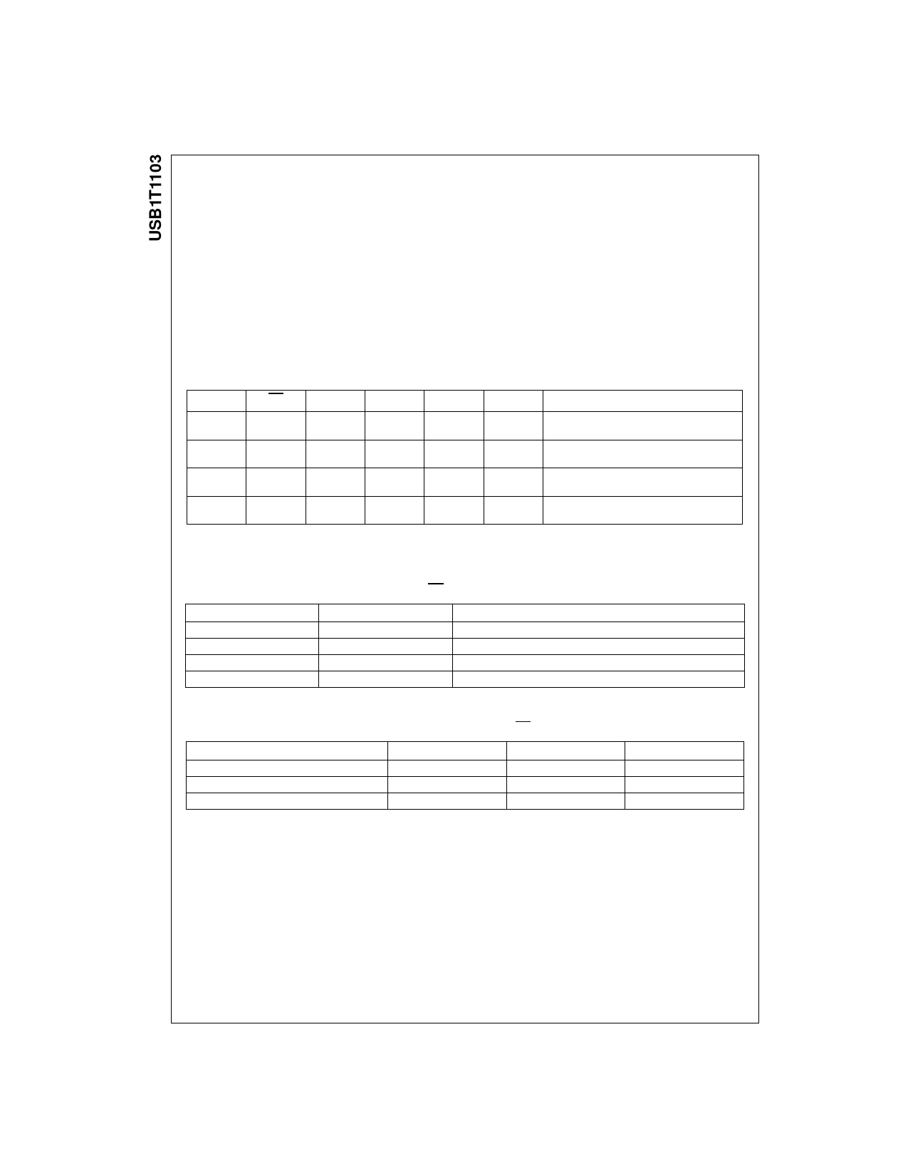
Functional Tables
Table 1. Function Select
SUSPND OE
D+, D-
RCV
Vp/Vpo Vm/Vmo
Function
L
L
Driving &
Active
Vpo Input
Vmo Input Normal Driving
Receiving
(Differential Receiver Active)
L
H
Receiving (1)
Active
Vp Output Vm Output Receiving
H
L
Driving
Inactive(2)
Vpo Input
Vmo Input Driving during Suspend
(Differential Receiver Inactive)
H
H
3 STATE(1)
Inactive(2)
Vp Output
Vm Output Low Power State
Notes:
1. Signal levels is function of connection and/or pull-up/pull-down resistors.
2. For SUSPND = HIGH mode the differential receiver is inactive and the output RCV is forced LOW. The out-of-suspend signaling
(K) is detected via the single-ended receivers of the Vp/Vpo and Vm/Vmo terminals.
Table 2. Driver Function (OE = L) using Differential Input Interface
Vm/Vmo
L
L
H
H
Notes:
3. SE0 = Single Ended Zero
Vp/Vpo
L
H
L
H
Data (D+ / D-)
SE0 (3)
Differential Logic 1
Differential Logic 0
Illegal State
Table 3. Receiver Function (OE = H)
D+, D-
RCV
Vp/Vpo
Vm/Vmo
Differential Logic 1
H
H
L
Differential Logic 0
L
L
H
SE0
X
L
L
Notes:
4. X = Don't Care
5. RCV(0) denotes the signal level on output RCV just prior to the SE0 or SE1 event. This level is stable during the SE0 or SE1
event period.
© 2005 Fairchild Semiconductor Corporation
USB1T1103 Rev. 1.0.3
4
www.fairchildsemi.com
Share Link: