NCV78M00 Просмотр технического описания (PDF) - ON Semiconductor
Номер в каталоге
Компоненты Описание
производитель
NCV78M00 Datasheet PDF : 14 Pages
| |||
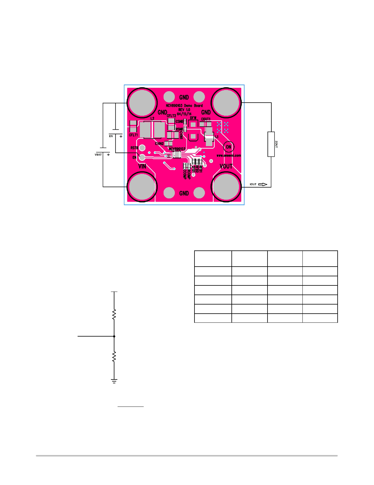
NCV890103GEVB
OPERATIONAL GUIDELINES
1. Connect a dc input voltage, within the 6.0 V to
36 V range, between VIN and GND.
2. Connect a dc enable voltage, within the 2.0 V to
36 V range, between EN and GND. This will
power up the switcher. The VOUT signal should
be 3.3 V.
3. Add a load to VOUT – up to 1.0 A.
Figure 5. NCV890103 Board Connections
ADDITIONAL GUIDELINES
Output Voltage Selection
The voltage output for the switcher is adjustable and can
be set with a resistor divider. The FB reference for the
switcher is 0.8 V.
VOUT
RUPPER
Desired
Output (V)
1.2
1.5
1.8
2.5
3.3
5.0
VREF (V)
0.8
0.8
0.8
0.8
0.8
0.8
RUPPER
(kW, 1%)
5.11
8.87
12.7
21.5
31.6
52.3
RLOWER
(kW, 1%)
10.0
10.0
10.0
10.0
10.0
10.0
FB = 0.8 V
RLOWER
Use the following equation:
RUPPER + RLOWER
VOUT*VFB
VFB
Some common setups are listed below:
Reset with Adjustable Delay
The RSTB pin is pulled low as long as the voltage on the
FB pin is lower than 92% (typical) of the reference voltage
(which corresponds to the output voltage being lower than
92% of its regulation level). It is high impedance when the
voltage goes above 94% (typical) of the regulation level,
after a delay adjusted by the capacitor on the DELAY pin.
The capacitor is held at ground until the output enters
regulation: CDELAY is then quickly charged to the internal
rail voltage (VRESU), then discharged by the Idelay current
until its voltage reaches the lower threshold VDELTH. Only
at this moment the RSTB pin voltage goes high, indicating
the end of the Reset condition.
http://onsemi.com
5
Share Link: 