VRE3021AD Просмотр технического описания (PDF) - Thaler Corporation
Номер в каталоге
Компоненты Описание
производитель
VRE3021AD Datasheet PDF : 8 Pages
| |||
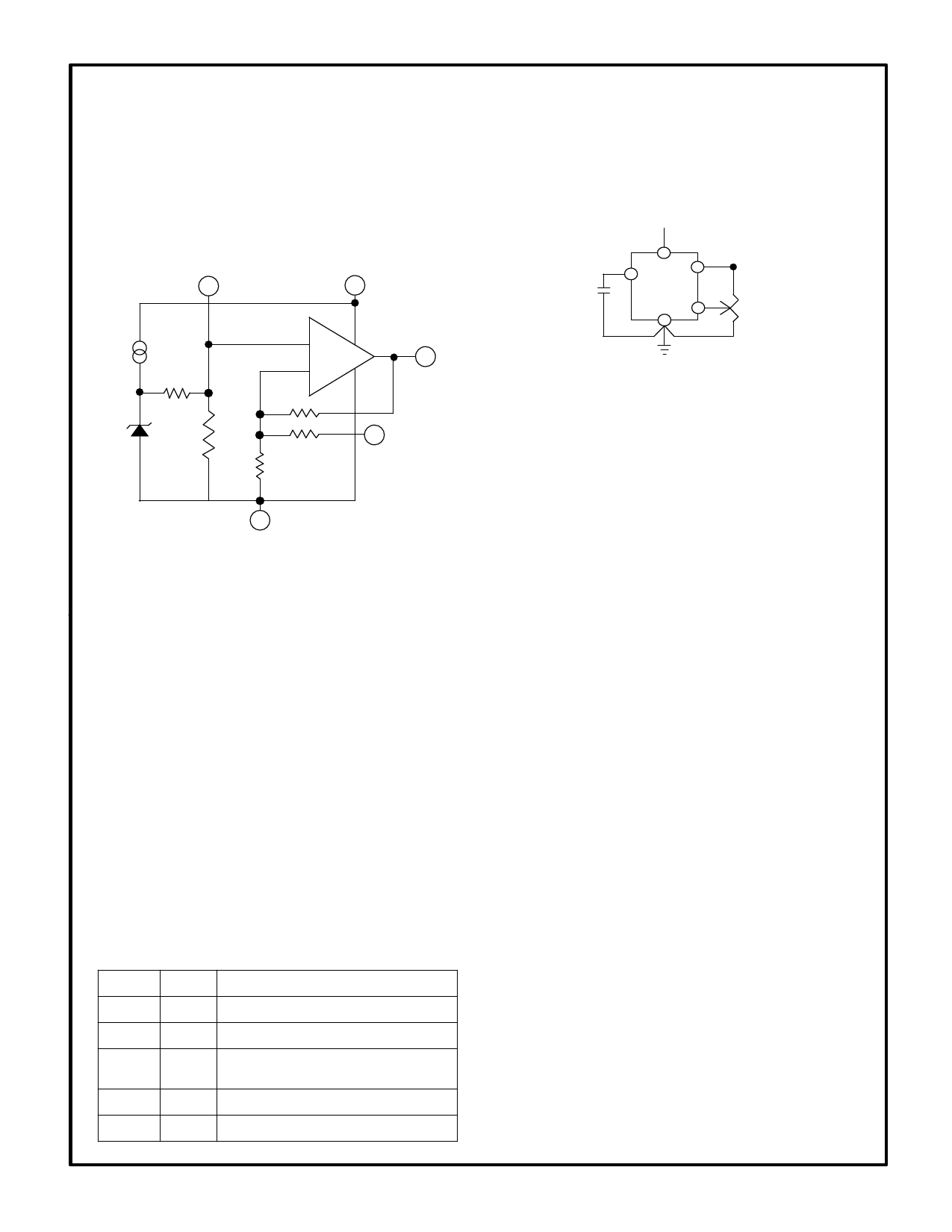
THEORY OF OPERATION
The following discussion refers to the schematic in
figure 2 below. A FET current source is used to bias a
6.3V zener diode. The zener voltage is divided by the
resistor network R1 and R2. This voltage is then applied
to the noninverting input of the operational amplifier which
amplifies the voltage to produce a 5.000V output. The
gain is determined by the resistor networks R3 and R4:
G=1 + R4/R3. The 6.3V zener diode is used because it is
the most stable diode over time and temperature.
8
2
R1
R2
+
6
-
R4
5
R3
4
Figure 2 Functional Block Diagram
The current source provides a closely regulated zener
current, which determines the slope of the references’
voltage vs. temperature function. By trimming the zener
current a lower drift over temperature can be achieved.
But since the voltage vs. temperature function is nonlinear
this compensation technique is not well suited for wide
temperature ranges.
Thaler Corporation has developed a nonlinear
compensation network of thermistors and resistors that is
used in the VRE series voltage references. This
proprietary network eliminates most of the nonlinearity in
the voltage vs. temperature function. By adjusting the
slope, Thaler Corporation produces a very stable voltage
over wide temperature ranges.
This network is less than 2% of the overall network
resistance so it has a negligible effect on long term
stability. Figure 3 shows the proper connection of the
VRE3050 series voltage references with the optional trim
resistor for initial error and the optional capacitor for noise
reduction.
PIN DESCRIPTION
1,3,7
2
4
5
6
8
N.C.
Vin
GND
TRIM
OUT
NR
Internally connected. Do not use
Positive power supply input
Ground
External trim input. Leave open if
not used.
Voltage reference output
Noise Reduction
BASIC CIRCUIT CONNECTION
Figure 3 shows the proper connection of the VRE3050
voltage reference with the optional trim resistor for initial
error and the optional capacitor for noise reduction.
CN 1µF
Optional Noise
Reduction
Capacitor
+ VIN
2
6
8
VRE3050
5
4
+ VOUT
10kΩ
Optional Fine
Trim Adjustment
Figure 3 External Connections
To achieve the specified performance, pay careful
attention to the layout. A low resistance star configuration
will reduce voltage errors, noise pickup, and noise
coupled from the power supply. Commons should be
connected to a single point to minimize interconnect
resistances.
VRE3050DS REV. D JULY 2000
Share Link: 