CXB1586AR Просмотр технического описания (PDF) - Sony Semiconductor
Номер в каталоге
Компоненты Описание
производитель
CXB1586AR Datasheet PDF : 18 Pages
| |||
CXB1586AR
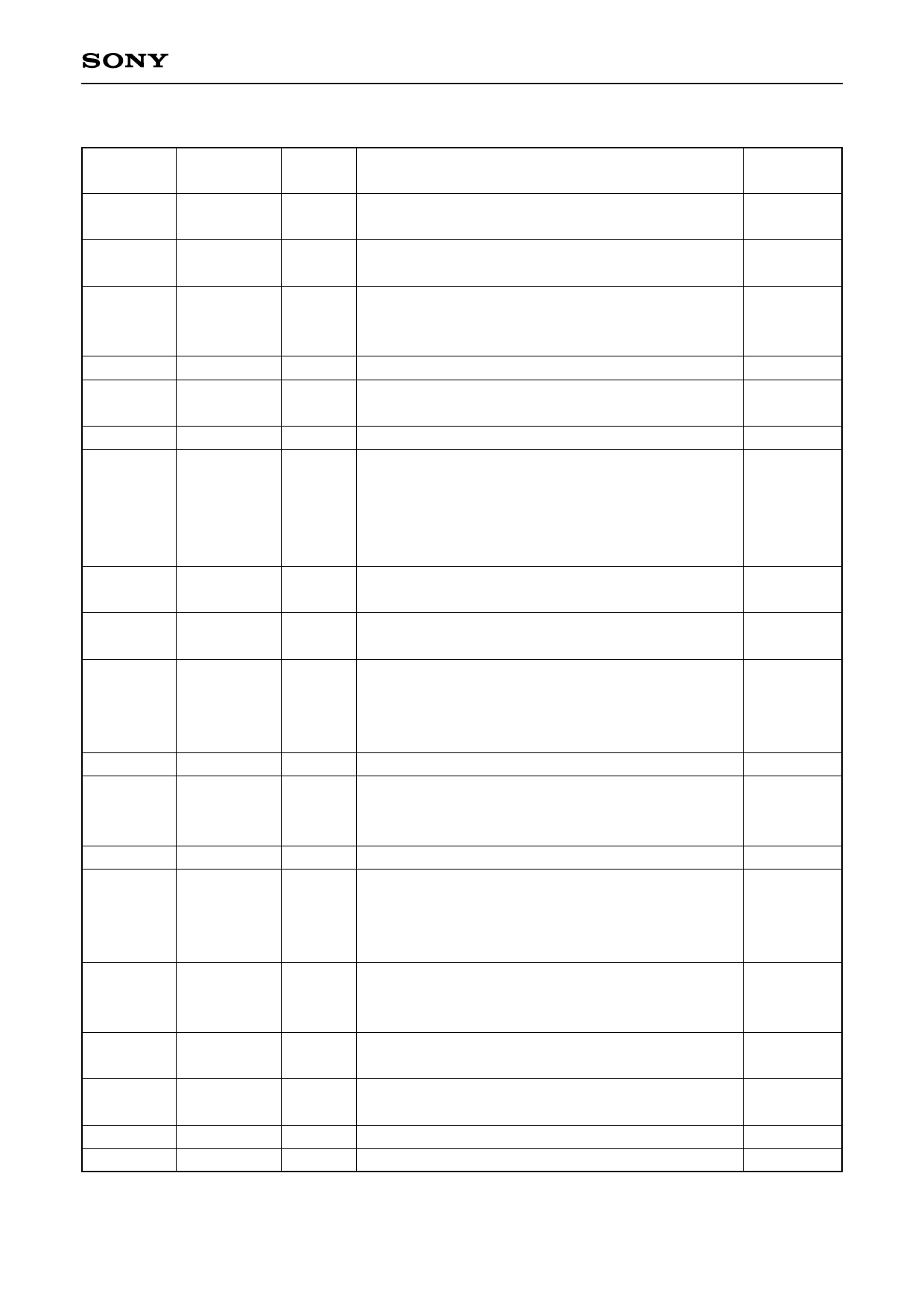
Pin description
Pin No.
1, 14, 32,
33, 46
2-4, 6-9,
11-13
5, 10, 20,
23, 28, 55,
57, 59
15
16
17
18
Symbol
VEET
TX0-9
VCCG
VEEP_TX
LPF_TX0
LPF_TX1
VCCP_TX
19
LBEN
21, 25,
56, 58
22
VEEG
REFCLK
24
BYTSYNCEN
26
TEST∗
27
LCKREF∗
29, 37, 42
VCCT
30
RBC1
31
RBC0
34-36,
38-41,
43-45
47
48
49
50
51
RX0-9
BYTSYNC
LPF_RX0
LPF_RX1
VCCP_RX
VEEP_RX
Type
PS
I_TTL
PS
PS
EX
PS
I_TTL
PS
I_TTL
I_TTL
I_TTL
I_TTL
PS
O_TTL
O_TTL
O_TTL
EX
PS
PS
Description
Equivalent
circuit
Ground for TTL output : Normally 0 V.
—
Parallel transmit data inputs to be serialized.
(a)
TX0 is serialized first and TX9 is last.
Power supply for internal logic gates :
—
Normally 3.3 V.
Ground for TX PLL : Normally 0 V.
—
Connect to external loop filter of TX PLL. Connect a
(e)
capacitor (0.01 µF) between LPF_TX0 and LPF_TX1.
Power supply for TX PLL : Normally 3.3 V.
—
Loop back enable : When high, TX serializer output
internally connects to RX deserializer input,
SDOUT/SDOUT∗ is held low/high, and SDIN/SDIN∗ is
(a)
disabled. When low, SDOUT/SDOUT∗ and
SDIN/SDIN∗ are enabled.
Power supply for internal logic gates :
—
Normally 0 V.
Reference clock for PLL and transmit byte clock
(a)
(106.25 MHz). Supplied by the host system.
Byte synchronization enable : When high, the positive
comma character (0011111) detection circuit is
(a)
enabled to establish byte synchronization (see Timing
Chart).
Test pin : Normally 3.3 V or open.
(a)
Lock to reference clock : An active low input.
LCKREF∗ forces the PLL lock to the REFCLK supplied
(a)
by the host system.
Power supply for TTL output : Normally 3.3 V.
—
Receive byte clocks recovered from the serial data
(53.125 MHz). These clocks are 180 degrees out of
(b)
phase, and RX0-9 are alternatively clocked on the
rising edge of these clocks (see Timing Chart)
Parallel receive data output :
(b)
RX0 is received first and RX9 is last.
Byte synchronization indicator : High when a positive
(b)
comma character is detected (see Timing Chart)
Connect to external loop filter of RX PLL. Connect a
(e)
capacitor (0.01 µF) between LPF_RX0 and LPF_RX1.
Power supply for RX PLL : Normally 3.3 V.
—
Ground for RX PLL : Normally 0 V.
—
—6—
Share Link: 