ML4662 Просмотр технического описания (PDF) - Micro Linear Corporation
Номер в каталоге
Компоненты Описание
производитель
ML4662 Datasheet PDF : 12 Pages
| |||
SYSTEM DESCRIPTION
Figure 1 shows a schematic diagram of the ML4662 in an
internal or external 10Base-FL MAU. On one side of the
transceiver is the AU interface and on the other is the fiber
optic interface. The AU interface is AC coupled when
used in an external transceiver or can be AC or DC
coupled when used in an internal transceiver. The AU
interface for an external transceiver includes isolation
transformers, some biasing resistors, and a voltage
regulator for power.
The fiber optic side of the transceiver requires an external
fiber optic transmitter, fiber optic receiver, and the
ML4622 or ML4624 fiber optic quantizers. The transmitter
uses a current driven output that directly drives the fiber
optic transmitter. The receive side of the transceiver
accepts the data after passing through the fiber optic
receiver and the ML4622/ML4624 fiber optic quantizer.
AU INTERFACE
The AUI interface consists of 3 pairs of signals: DO, CI,
and DI (Figure 1). The DO pair contains transmit data
from the DTE which is received by the transceiver and
sent out onto the fiber optic cable. The DI pair contains
valid data that has been either received from the fiber
optic cable or looped back from the DO, and output
through the DI pair to the DTE. The CI pair indicates
whether a collision has occurred. It is an output that
oscillates at 10MHz if a collision Jabber or SQE Test has
taken place, otherwise it remains idle.
When the transceiver is external, these three pairs are AC
coupled through isolation transformers, while an internal
transceiver may be AC or DC coupled. For the AC
coupled interface, DO (which is an input) must be DC
biased (shifted up in voltage) for the proper common
mode input voltage. The BIAS pin serves this purpose.
When DC coupled, the transmit pair coming from the
serial interface provides this common mode voltage, and
the BIAS pin is not connected.
The two 39Ω 1% resistors tied to the Tx+ and Tx– pins
provide a point to connect the common mode bias voltage
as discussed above, and they provide the proper matching
termination for the AUI cable. The CI and DI pair, which
are output from the transceiver to the AUI cable, require
360Ω pull down resistors when terminated with a 78Ω
load. However on a DTE card, CI and DI do not need 78Ω
terminating resistors. This also means that the pull down
resistors on CI and DI can be 1kΩ or greater depending
upon the particular Manchester encoder/decoder chip
used. Using higher value pull down resistors as in a DTE
card will save power.
The AUI drivers are capable of driving the full 50 meters
of cable length and have a rise and fall time of typically
4ns. In the idle state, the outputs go to the same voltage to
prevent DC standing current in the isolation transformers.
ML4662
TRANSMISSION
The transmit function consists of detecting the presence of
data from the AUI DO input (Tx+, Tx–) and driving that data
onto the fiber optic LED transmitter. A positive signal on the
Tx+ lead relative to the Tx– lead of the DO circuit will result
in no current, hence the fiber optic LED is in a low light
condition. When Tx+ is more negative than Tx–, the ML4662
will sink current into the chip and the LED will light up.
Before data will be transmitted onto the fiber optic cable
from the AUI interface, it must exceed the squelch
requirements for the DO pair. The Tx squelch circuit serves
the function of preventing any noise from being transmitted
onto the fiber. This circuit rejects signals with pulse widths
less than typically 20ns (negative going), or with levels less
than –250mV. Once Tx squelch circuit has unsquelched, it
looks for the start of idle signal to turn on the squelch circuit
again. The transmitter turns on the squelch again when it
receives an input signal at TxIN± that is more positive than
–250mV for more than approximately 180ns.
At the start of a packet transmission, no more than 2 bits are
received from the DO circuit, and are not transmitted onto
the fiber optic cable. The difference between start-up delays
(bit loss plus steady-state propagation delay) for any two
packets that are separated by 9.6µs or less will not exceed
200ns.
FIBER OPTIC LED DRIVER
The output stage of the transmitter is a current mode
switch which develops the output light by sinking current
through the LED into the TxOUT pin. Once the current
requirement for the LED is determined, the RTSET resistor
is selected. The following equation is used to select the
correct RTSET resistor:
RTSET
=
52mA
IOUT
162Ω
(1)
The transmitter enters the idle state when it detects start of
idle on Tx+ and Tx– input pins. After detection, the
transmitter switches to a 1MHz output idle signal.
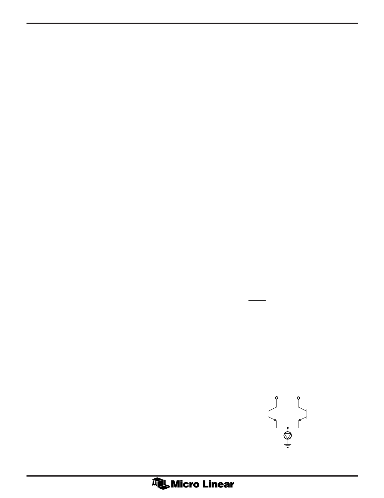
The output current is switched through the TxOUT pin
during the on cycle and through the VCCTx pin during the
off cycle (Figure 2). Since the sum of the current in these
two pins is constant, VCCTx should be connected as close
as possible to the VCC connection for the LED (Figure 2).
VCCTx TxOUT
IOUT
Figure 2. Fiber Optic LED Driver Structure.
7
Share Link: 