ML4662 Просмотр технического описания (PDF) - Micro Linear Corporation
Номер в каталоге
Компоненты Описание
производитель
ML4662 Datasheet PDF : 12 Pages
| |||
ML4662
ABSOLUTE MAXIMUM RATINGS
Absolute maximum ratings are those values beyond which
the device could be permanently damaged. Absolute
maximum ratings are stress ratings only and functional
device operation is not implied.
Power Supply Voltage Range
VCC .................................................... GND –0.3 to 6V
Input Voltage Range
Digital Inputs (SQEN, LMONIN, LBDIS)
.............................................. GND –0.3 to VCC + 0.3V
Tx+, Tx–, RxIN+, RxIN– ........ GND –0.3 to VCC + 0.3V
Input Current
RRSET, RTSET, JAB, CLSN, XMT, RCV, LMON ..... 60mA
Output Current
TxOUT ............................................................... 70mA
Junction Temperature ............................................. 150°C
Storage Temperature Range ..................... –65°C to 150°C
Lead Temperature (Soldering) ................................. 260°C
Thermal Resistance (θJA) ...................................... 68°C/W
OPERATING CONDITIONS
Supply Voltage (VCC) ........................................... 5V ± 5%
LED on Current ....................................................... 10mA
RRSET .......................................................... 61.9kΩ ± 1%
RTSET ............................................................. 162Ω ± 1%
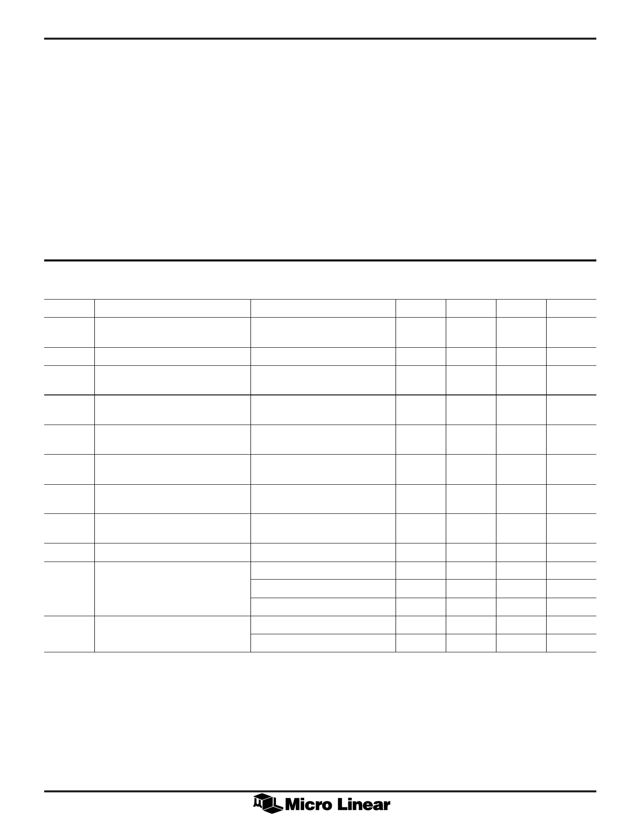
ELECTRICAL CHARACTERISTICS
Unless otherwise specified, TA = Operating Temperature Range, VCC = 5V ± 10% (Note 1)
SYMBOL
PARAMETER
CONDITIONS
MIN
TYP
ICC
Power Supply Current
While Transmitting
VCC = 5V, RTSET = 162Ω
(Note 2)
VOL
IOUT
VSQ
LED Drivers
Transmit Peak Output Current
Transmit Squelch Voltage Level
(Tx+, Tx–)
IOL = 10mA (Note 3)
RTSET = 162Ω,
VCC = VCCTx = 5V ±5% (Note 4)
47
–300
52
–250
VINCM Common mode Input Voltage
2
(Tx±, RxIN±)
VDO
Differential Output Voltage
(Rx±, COL±)
±550
VCM
Common Mode
4.0
Output Voltage (Rx±, COL±)
VDOO
Differential Output
Voltage Imbalance (Rx±, COL±)
VBIAS
VSQE
BIAS Voltage
SQE/JABD
SQE Test Disable
Both Disabled
3.2
1.5
VLBTH LBDIS Threshold
Both Enabled
Disabled
Enabled
VCC – 0.5
VCC – 0.10
MAX
200
UNITS
mA
0.8
V
60
mA
–200
mV
VCC – 0.5
V
±1200
mV
V
±40
mV
V
0.3
V
VCC – 2
V
V
V
1
V
4
Share Link: 