ADN4697EBRZ Просмотр технического описания (PDF) - Analog Devices
Номер в каталоге
Компоненты Описание
производитель
ADN4697EBRZ Datasheet PDF : 20 Pages
| |||
ADN4691E/ADN4693E/ADN4696E/ADN4697E
Data Sheet
ABSOLUTE MAXIMUM RATINGS
TA = TMIN to TMAX, unless otherwise noted.
Table 6.
Parameter
VCC
Digital Input Voltage (DE, RE, DI)
Receiver Input (A, B) Voltage
Half-Duplex (ADN4691E, ADN4696E)
Full-Duplex (ADN4693E, ADN4697E)
Receiver Output Voltage (RO)
Driver Output (A, B, Y, Z) Voltage
ESD Rating (A, B, Y, Z Pins)
HBM (Human Body Model)
Air Discharge
Contact Discharge
IEC 61000-4-2, Air Discharge
IEC 61000-4-2, Contact Discharge
ESD Rating (Other Pins, HBM)
ESD Rating (All Pins)
FICDM
Operating Temperature Range
Storage Temperature Range
Rating
−0.5 V to +4 V
−0.5 V to +4 V
−1.8 V to +4 V
−4 V to +6 V
−0.3 V to +4 V
−1.8 V to +4 V
±15 kV
±8 kV
±10 kV
±8 kV
±4 kV
±1.25 kV
−40°C to +85°C
−65°C to +150°C
Stresses at or above those listed under Absolute Maximum
Ratings may cause permanent damage to the product. This is a
stress rating only; functional operation of the product at these
or any other conditions above those indicated in the operational
section of this specification is not implied. Operation beyond
the maximum operating conditions for extended periods may
affect product reliability.
THERMAL RESISTANCE
θJA is specified for the worst case conditions, that is, a device
soldered in a circuit board for surface-mount packages.
Table 7. Thermal Resistance
Package Type
θJA
8-Lead SOIC
121
14-Lead SOIC
86
Unit
°C/W
°C/W
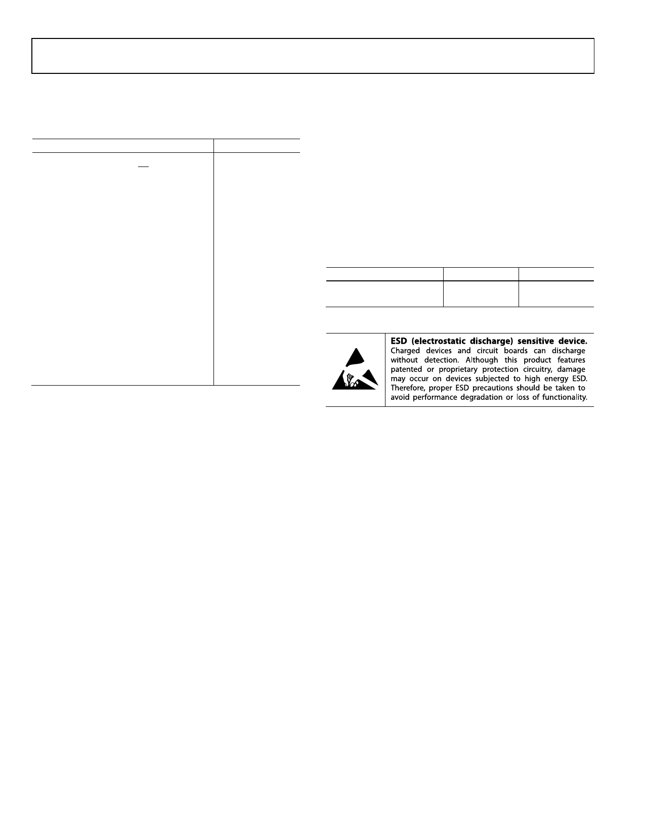
ESD CAUTION
Rev. B | Page 6 of 20
Share Link: 