ADN4690EBRZ-RL7(RevA) Просмотр технического описания (PDF) - Analog Devices
Номер в каталоге
Компоненты Описание
производитель
ADN4690EBRZ-RL7
(Rev.:RevA)
(Rev.:RevA)
Analog Devices

ADN4690EBRZ-RL7 Datasheet PDF : 20 Pages
| |||
Data Sheet
ADN4690E/ADN4692E/ADN4694E/ADN4695E
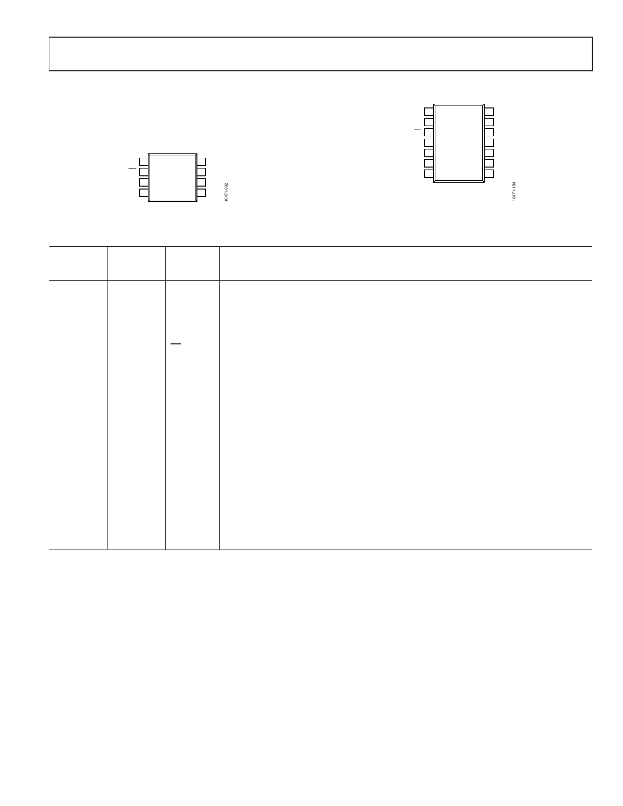
PIN CONFIGURATIONS AND FUNCTION DESCRIPTIONS
RO 1 ADN4690E/ 8 VCC
RE 2 ADN4694E 7 B
DE 3 TOP VIEW 6 A
DI 4 (Not to Scale) 5 GND
Figure 3. ADN4690E/ADN4694E Pin Configuration
NC 1
14 VCC
RO 2 ADN4692E/ 13 VCC
RE 3 ADN4695E 12 A
DE 4
TOP VIEW
11 B
DI 5 (Not to Scale) 10 Z
GND 6
9Y
GND 7
8 NC
NOTES
1. NC = NO CONNECT. DO NOT
CONNECT TO THIS PIN.
Figure 4. ADN4692E/ADN4695E Pin Configuration
Table 8. Pin Function Descriptions
ADN4690E/ ADN4692E/
ADN4694E ADN4695E
Pin No.
Pin No.
Mnemonic
1
2
RO
2
3
RE
3
4
DE
4
5
DI
5
6, 7
GND
N/A
9
Y
N/A
10
Z
6
N/A
A
N/A
12
A
7
N/A
B
N/A
11
B
8
13, 14
VCC
N/A
1, 8
NC
Description
Receiver Output. Type 1 receiver (ADN4690E/ADN4692E), when enabled:
If A − B ≥ 50 mV, then RO = logic high. If A − B ≤ −50 mV, then RO = logic low.
Type 2 receiver (ADN4694E/ADN4695E), when enabled:
If A − B ≥ 150 mV, then RO = logic high. If A − B ≤ 50 mV, then RO = logic low.
Receiver output is undefined outside these conditions.
Receiver Output Enable. A logic low on this pin enables the receiver output, RO.
A logic high on this pin places RO in a high impedance state.
Driver Output Enable. A logic high on this pin enables the driver differential outputs.
A logic low on this pin places the driver differential outputs in a high impedance state.
Driver Input. Half-duplex (ADN4690E/ADN4694E), when enabled:
A logic low on DI forces A low and B high, whereas a logic high on DI forces A high and B low.
Full-duplex (ADN4692E/ADN4695E), when enabled:
A logic low on DI forces Y low and Z high, whereas a logic high on DI forces Y high and Z low.
Ground.
Noninverting Driver Output Y.
Inverting Driver Output Z.
Noninverting Receiver Input A and Noninverting Driver Output A.
Noninverting Receiver Input A.
Inverting Receiver Input B and Inverting Driver Output B.
Inverting Receiver Input B.
Power Supply (3.3 V ± 0.3 V).
No Connect. Do not connect to these pins.
Rev. A | Page 7 of 20
Share Link: