ADN4690EBRZ(RevA) Просмотр технического описания (PDF) - Analog Devices
Номер в каталоге
Компоненты Описание
производитель
ADN4690EBRZ
(Rev.:RevA)
(Rev.:RevA)
Analog Devices

ADN4690EBRZ Datasheet PDF : 20 Pages
| |||
Data Sheet
3.3 V, 100 Mbps, Half- and Full-Duplex,
High Speed M-LVDS Transceivers
ADN4690E/ADN4692E/ADN4694E/ADN4695E
FEATURES
Multipoint LVDS transceivers (low voltage differential
signaling driver and receiver pairs)
Switching rate: 100 Mbps (50 MHz)
Supported bus loads: 30 Ω to 55 Ω
Choice of 2 receiver types
Type 1 (ADN4690E/ADN4692E): hysteresis of 25 mV
Type 2 (ADN4694E/ADN4695E): threshold offset of 100 mV
for open-circuit and bus-idle fail-safe
Conforms to TIA/EIA-899 standard for M-LVDS
Glitch-free power-up/power-down on M-LVDS bus
Controlled transition times on driver output
Common-mode range: −1 V to +3.4 V, allowing
communication with 2 V of ground noise
Driver outputs high-Z when disabled or powered off
Enhanced ESD protection on bus pins
±15 kV HBM (human body model), air discharge
±8 kV HBM (human body model), contact discharge
±10 kV IEC 61000-4-2, air discharge
±8 kV IEC 61000-4-2, contact discharge
Operating temperature range: −40°C to +85°C
Available in 8-lead (ADN4690E/ADN4694E) and 14-lead
(ADN4692E/ADN4695E) SOIC packages
APPLICATIONS
Backplane and cable multipoint data transmission
Multipoint clock distribution
Low power, high speed alternative to shorter RS-485 links
Networking and wireless base station infrastructure
GENERAL DESCRIPTION
The ADN4690E/ADN4692E/ADN4694E/ADN4695E are
multipoint, low voltage differential signaling (M-LVDS)
transceivers (driver and receiver pairs) that can operate at up
to 100 Mbps (50 MHz). Slew rate control is implemented on the
driver outputs. The receivers detect the bus state with a differential
input of as little as 50 mV over a common-mode voltage range of
−1 V to +3.4 V. ESD protection of up to ±15 kV is implemented
on the bus pins. The parts adhere to the TIA/EIA-899 standard for
M-LVDS and complement TIA/EIA-644 LVDS devices with
additional multipoint capabilities.
The ADN4690E/ADN4692E are Type 1 receivers with 25 mV of
hysteresis, so that slow-changing signals or loss of input does
not lead to output oscillations. The ADN4694E/ADN4695E are
Type 2 receivers exhibiting an offset threshold, guaranteeing the
output state when the bus is idle (bus-idle fail-safe) or the
inputs are open (open-circuit fail-safe).
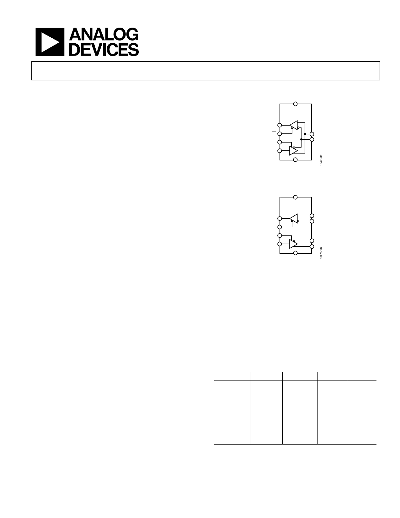
FUNCTIONAL BLOCK DIAGRAMS
VCC
ADN4690E/
ADN4694E
RO
R
RE
A
B
DE
DI
D
GND
Figure 1.
VCC
ADN4692E/
ADN4695E
RO
R
A
B
RE
DE
Z
DI
D
Y
GND
Figure 2.
The parts are available as half-duplex in an 8-lead SOIC package
(the ADN4690E/ADN4694E) or as full-duplex in a 14-lead
SOIC package (the ADN4692E/ADN4695E). A selection table
for the ADN469xE parts is shown in Table 1.
Table 1. ADN469xE Selection Table
Part No. Receiver Data Rate
ADN4690E Type 1
100 Mbps
ADN4691E Type 1
200 Mbps
ADN4692E Type 1
100 Mbps
ADN4693E Type 1
200 Mbps
ADN4694E Type 2
100 Mbps
ADN4695E Type 2
100 Mbps
ADN4696E Type 2
200 Mbps
ADN4697E Type 2
200 Mbps
SOIC
8-lead
8-lead
14-lead
14-lead
8-lead
14-lead
8-lead
14-lead
Duplex
Half
Half
Full
Full
Half
Full
Half
Full
Rev. A
Information furnished by Analog Devices is believed to be accurate and reliable. However, no
responsibility is assumed by Analog Devices for its use, nor for any infringements of patents or other
rights of third parties that may result from its use. Specifications subject to change without notice. No
license is granted by implication or otherwise under any patent or patent rights of Analog Devices.
Trademarks and registered trademarks are the property of their respective owners.
One Technology Way, P.O. Box 9106, Norwood, MA 02062-9106, U.S.A.
Tel: 781.329.4700
www.analog.com
Fax: 781.461.3113
©2012 Analog Devices, Inc. All rights reserved.
Share Link: