LHF16KAP –ü—Ä–æ—Å–º–æ—Ç—Ä —Ç–µ—Ö–Ω–∏—á–µ—Å–∫–æ–≥–æ –æ–ø–∏—Å–∞–Ω–∏—è (PDF) - Sharp Electronics
–ù–æ–º–µ—Ä –≤ –∫–∞—Ç–∞–ª–æ–≥–µ
–ö–æ–º–ø–æ–Ω–µ–Ω—Ç—ã –û–ø–∏—Å–∞–Ω–∏–µ
–ø—Ä–æ–∏–∑–≤–æ–¥–∏—Ç–µ–ª—å
LHF16KAP Datasheet PDF : 64 Pages
| |||
sharp
LHF16KAP
5
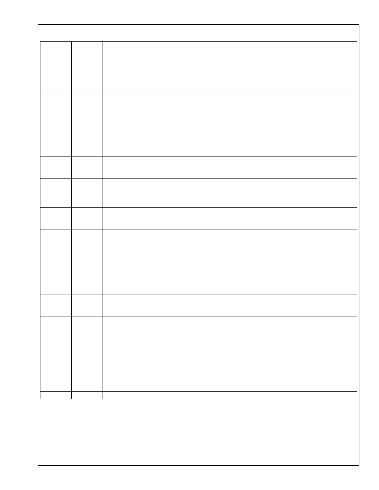
Table 2. Pin Descriptions
Symbol Type
Name and Function
ADDRESS INPUTS: Inputs for addresses during read and write operations. Addresses are
internally latched during a write cycle.
A0-A20
INPUT
A0: Byte Select Address. Not used in x16 mode(can be floated).
A1-A4: Column Address. Selects 1 of 16 bit lines.
A5-A15: Row Address. Selects 1 of 2048 word lines.
A16-A20 : Block Address.
DATA INPUT/OUTPUTS:
DQ0-DQ7:Inputs data and commands during CUI write cycles; outputs data during memory
array, status register, query, and identifier code read cycles. Data pins float to high-
DQ0-DQ15
INPUT/
OUTPUT
impedance when the chip is deselected or outputs are disabled. Data is internally latched
during a write cycle.
DQ8-DQ15:Inputs data during CUI write cycles in x16 mode; outputs data during memory
array read cycles in x16 mode; not used for status register, query and identifier code read
mode. Data pins float to high-impedance when the chip is deselected, outputs are
CE0#,
CE1#
INPUT
disabled, or in x8 mode(Byte#=VIL). Data is internally latched during a write cycle.
CHIP ENABLE: Activates the device’s control logic, input buffers decoders, and sense
amplifiers. Either CE0# or CE1# VIH deselects the device and reduces power consumption
to standby levels. Both CE0# and CE1# must be VIL to select the devices.
RESET/DEEP POWER-DOWN: Puts the device in deep power-down mode and resets
RP#
INPUT
internal automation. RP# VIH enables normal operation. When driven VIL, RP# inhibits
write operations which provides data protection during power transitions. Exit from deep
power-down sets the device to read array mode.
OE# INPUT OUTPUT ENABLE: Gates the device’s outputs during a read cycle.
WE#
INPUT
WRITE ENABLE: Controls writes to the CUI and array blocks. Addresses and data are
latched on the rising edge of the WE# pulse.
STS (RY/BY#): Indicates the status of the internal WSM. When configured in level mode
(default mode), it acts as a RY/BY# pin. When low, the WSM is performing an internal
OPEN operation (block erase, full chip erase, (multi) word/byte write or block lock-bit
STS DRAIN configuration). STS High Z indicates that the WSM is ready for new commands, block
OUTPUT erase is suspended, and (multi) word/byte write is inactive, (multi) word/byte write is
suspended or the device is in deep power-down mode. For alternate configurations of the
STATUS pin, see the Configuration command.
WP#
INPUT
WRITE PROTECT: Master control for block locking. When VIL, Locked blocks can not be
erased and programmed, and block lock-bits can not be set and reset.
BYTE#
BYTE ENABLE: BYTE# VIL places device in x8 mode. All data is then input or output on
INPUT DQ0-7, and DQ8-15 float. BYTE# VIH places the device in x16 mode , and turns off the A0
input buffer.
BLOCK ERASE, FULL CHIP ERASE, (MULTI) WORD/BYTE WRITE, BLOCK LOCK-
BIT CONFIGURATION POWER SUPPLY: For erasing array blocks, writing bytes or
VPP SUPPLY configuring block lock-bits. With VPP≤VPPLK, memory contents cannot be altered. Block
erase, full chip erase, (multi) word/byte write and block lock-bit configuration with an invalid
VPP (see DC Characteristics) produce spurious results and should not be attempted.
DEVICE POWER SUPPLY: Internal detection configures the device for 5V operation. Do
VCC
SUPPLY not float any power pins. With VCC≤VLKO, all write attempts to the flash memory are
inhibited. Device operations at invalid VCC voltage (see DC Characteristics) produce
spurious results and should not be attempted.
GND SUPPLY GROUND: Do not float any ground pins.
NC
NO CONNECT: Lead is not internal connected; it may be driven or floated.
Rev. 2.0
Share Link: 