ADM1270CP-EVALZ(Rev0) Просмотр технического описания (PDF) - Analog Devices
Номер в каталоге
Компоненты Описание
производитель
ADM1270CP-EVALZ Datasheet PDF : 22 Pages
| |||
ADM1270
Data Sheet
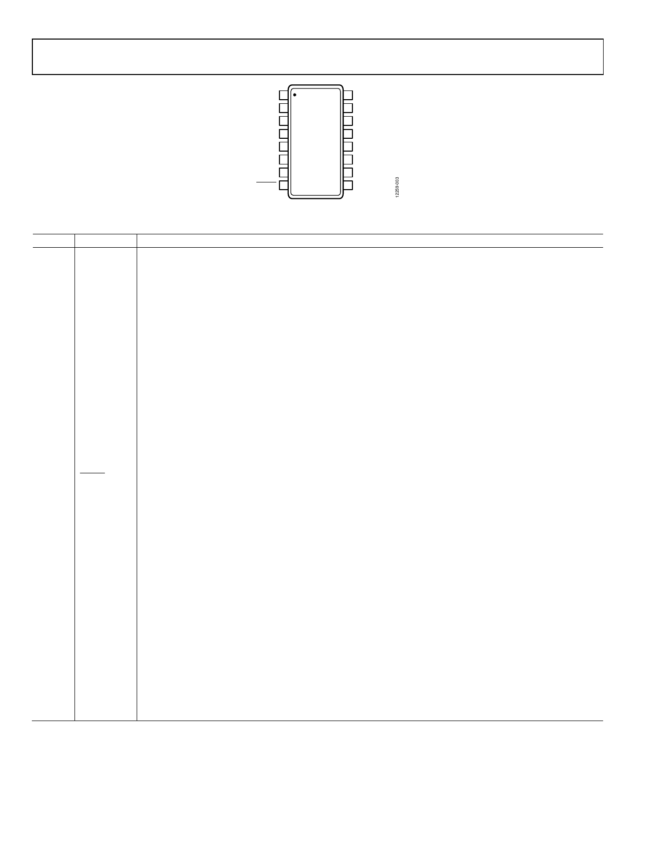
VCC/SENSE+ 1
RPFG 2
VCAP 3
ISET 4
UV 5
OV 6
ENABLE 7
FAULT 8
16 SENSE–
15 GATE
ADM1270
TOP VIEW
(Not to Scale)
14 PWRGD
13 FLB
12 FB_PG
11 TIMER_OFF
10 TIMER
9 GND
Figure 3. 16-Lead QSOP Pin Configuration
Table 5. 16-Lead QSOP Pin Function Descriptions
Pin No. Mnemonic Description
1
VCC/SENSE+ Positive Supply Input Pin (VCC). A UVLO circuit resets the device when a low supply voltage is detected. GATE is
held off when the supply is below UVLO. No sequencing is required.
Positive Current Sense Input Pin (SENSE+). This pin connects to the main supply input. A sense resistor between
the VCC/SENSE+ pin and the SENSE− pin sets the analog current limit. The hot swap operation of the ADM1270
controls the external FET gate to maintain the sense voltage (VSENSE+ − VSENSE−).
2
RPFG
Reverse Protection FET Gate Driver Output. Connect this pin to the gate of the external reverse polarity protection
P-channel FET for low voltage drop operation.
3
VCAP
Internal Regulated Supply. Place a capacitor with a 1 µF or greater value on this pin to maintain good accuracy.
This pin can be used as a reference to program the ISET pin voltage.
4
ISET
Current Limit. This pin allows the current-limit threshold to be programmed. The default limit is set when this pin
is connected directly to VCAP. To achieve a user defined sense voltage, the current limit can be adjusted using a
resistor divider from VCAP. An external reference can also be used.
5
UV
Undervoltage Input Pin. An external resistor divider is connected from the supply to this pin to allow an internal
comparator to detect whether the supply is under the UV limit.
6
OV
Overvoltage Input Pin. An external resistor divider is connected from the supply to this pin to allow an internal
comparator to detect whether the supply is above the OV limit.
7
ENABLE
Enable Pin. This pin is a digital logic input. This input must be high to allow the ADM1270 controller to begin a
power-up sequence. If this pin is held low, the ADM1270 is prevented from powering up. There is no internal pull-
up on this pin.
8
FAULT
Fault Output. This pin indicates that the device has shut down due to an overcurrent fault condition. The device
can be configured for automatic retry after shutdown by connecting this pin directly to the ENABLE pin.
9
GND
Ground Pin.
10
TIMER
Timer Pin. An external capacitor, CTIMER, sets an SOA overcurrent fault delay. The GATE pin is pulled off when the
voltage on the TIMER pin exceeds the upper threshold.
11
TIMER_OFF Timer Off Pin. An external capacitor, CTIMER_OFF, sets an initial timing cycle delay and the SOA off time delay. After an
SOA overcurrent fault has occurred, the GATE pin is pulled off until the voltage on the TIMER_OFF pin exceeds the
threshold.
12
FB_PG
PWRGD Feedback Input Pin. An external resistor divider is connected from the output voltage to this pin to allow
an internal comparator to detect when the output voltage is above the PWRGD threshold.
13
FLB
Foldback Pin. A foldback resistor divider is placed from the source of the FET to this pin. Foldback reduces the
current limit when the source voltage drops. The foldback feature ensures that the power through the FET is not
increased beyond the SOA limits.
14
PWRGD
Power-Good Signal. This signal indicates that the supply is within tolerance. This signal is based on the voltage
present on the FB_PG pin.
15
GATE
Gate Output Pin. This pin is the gate drive of an external P-channel FET. This pin is driven by the FET drive
controller, which provides a pull-down current to charge the FET gate pin. The FET drive controller regulates to a
maximum load current by regulating the GATE pin. GATE is held off when the supply is below UVLO.
16
SENSE−
Negative Current Sense Input Pin. A sense resistor between the VCC/SENSE+ pin and the SENSE− pin sets the
analog current limit. The hot swap operation of the ADM1270 controls the external FET gate to maintain the sense
voltage (VSENSE+ − VSENSE−). This pin also connects to the FET drain pin.
Rev. 0 | Page 8 of 21
Share Link: 