CAT25080YI-G Просмотр технического описания (PDF) - ON Semiconductor
Номер в каталоге
Компоненты Описание
производитель
CAT25080YI-G Datasheet PDF : 18 Pages
| |||
CAT25080, CAT25160
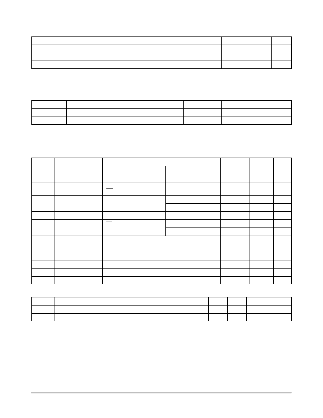
Table 1. ABSOLUTE MAXIMUM RATINGS
Parameters
Ratings
Units
Operating Temperature
−45 to +130
°C
Storage Temperature
−65 to +150
°C
Voltage on any Pin with Respect to Ground (Note 1)
−0.5 to VCC + 0.5
V
Stresses exceeding those listed in the Maximum Ratings table may damage the device. If any of these limits are exceeded, device functionality
should not be assumed, damage may occur and reliability may be affected.
1. The DC input voltage on any pin should not be lower than −0.5 V or higher than VCC + 0.5 V. During transitions, the voltage on any pin may
undershoot to no less than −1.5 V or overshoot to no more than VCC + 1.5 V, for periods of less than 20 ns.
Table 2. RELIABILITY CHARACTERISTICS (Note 2)
Symbol
Parameter
Min
Units
NEND (Note 3) Endurance
1,000,000
Program / Erase Cycles
TDR
Data Retention
100
Years
2. These parameters are tested initially and after a design or process change that affects the parameter according to appropriate AEC−Q100
and JEDEC test methods.
3. Page Mode, VCC = 5 V, 25°C.
Table 3. D.C. OPERATING CHARACTERISTICS
(VCC = 1.8 V to 5.5 V, TA = −40°C to +85°C and VCC = 2.5 V to 5.5 V, TA = −40°C to +125°C unless otherwise specified.)
Symbol
Parameter
Test Conditions
Min
Max
ICC
Supply Current
Read, Write, VCC = 5.0 V,
10 MHz / −40°C to +85°C
2
SO open
5 MHz / −40°C to +125°C
2
ISB1
ISB2
IL
ILO
VIL
VIH
VOL1
VOH1
VOL2
VOH2
Standby Current
Standby Current
Input Leakage Current
Output Leakage
Current
Input Low Voltage
Input High Voltage
Output Low Voltage
Output High Voltage
Output Low Voltage
Output High Voltage
VIN = GND or VCC, CS = VCC,
WP = VCC, VCC = 5.0 V
VIN = GND or VCC, CS = VCC,
WP = GND, VCC = 5.0 V
VIN = GND or VCC
CS = VCC,
VOUT = GND or VCC
VCC > 2.5 V, IOL = 3.0 mA
VCC > 2.5 V, IOH = −1.6 mA
VCC > 1.8 V, IOL = 150 mA
VCC > 1.8 V, IOH = −100 mA
TA = −40°C to +85°C
TA = −40°C to +125°C
TA = −40°C to +85°C
TA = −40°C to +125°C
2
−2
−1
−1
−0.5
0.7 VCC
VCC − 0.8 V
VCC − 0.2 V
4
5
2
1
2
0.3 VCC
VCC + 0.5
0.4
0.2
Units
mA
mA
mA
mA
mA
mA
mA
mA
V
V
V
V
V
V
Table 4. PIN CAPACITANCE (Note 2) (TA = 25°C, f = 1.0 MHz, VCC = +5.0 V)
Symbol
Test
Conditions
COUT
CIN
Output Capacitance (SO)
Input Capacitance (CS, SCK, SI, WP, HOLD)
VOUT = 0 V
VIN = 0 V
Min
Typ
Max
Units
8
pF
8
pF
www.onsemi.com
2
Share Link: 