MC141516 Просмотр технического описания (PDF) - Motorola => Freescale
Номер в каталоге
Компоненты Описание
производитель
MC141516 Datasheet PDF : 16 Pages
| |||
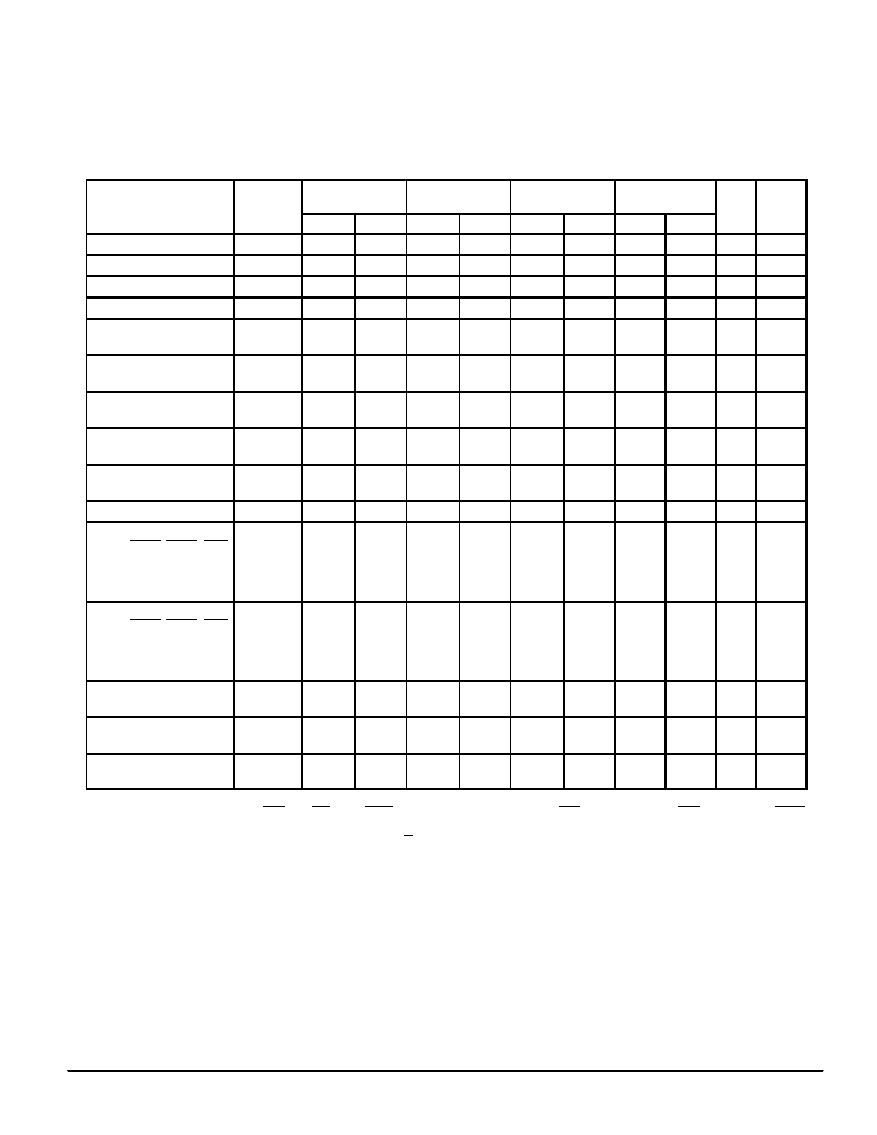
AC OPERATING CONDITIONS AND CHARACTERISTICS
(VDD = 3.3 V + 10%, – 5%, TA = 0 to 70°C, Unless Otherwise Noted)
Input Timing Measurement Reference Level . . . . . . . . . . . . . . 1.25 V
Input Pulse Levels . . . . . . . . . . . . . . . . . . . . . . . . . . . . . . . . . 0 to 2.5 V
Input Rise/Fall Time . . . . . . . . . . . . . . . . . . . . . . 1.0 V/ns (20 to 80%)
Output Timing Reference Level . . . . . . . . . . . . . . . . . . . . . . . . . 1.25 V
Output Load . . . . . . . . . . . . . . See Figure 2 Unless Otherwise Noted
READ/WRITE CYCLE TIMING (See Notes 1 through 4)
Parameter
Cycle Time
Clock High Pulse Width
Clock Low Pulse Width
Clock Access Time
Output Enable to Output
Valid
Symbol
tKHKH
tKHKL
tKLKH
tKHQV
tGLQV
63P733A–133
133 MHz
Min
Max
7.5
—
3
—
3
—
—
4
—
3.8
63P733A–117
117 MHz
Min
Max
8.5
—
3.4
—
3.4
—
—
4.2
—
3.8
63P733A–100
100 MHz
Min
Max
10
—
4
—
4
—
—
4.5
—
4.5
63P733A–90
90 MHz
Min
Max
11
—
4.4
—
4.4
—
—
5
—
5
Unit Notes
ns
ns
ns
ns
ns
Clock High to Output
Active
tKHQX1
0
—
0
—
0
—
0
—
ns
5, 6
Clock High to Output
Change
tKHQX2
1.5
—
1.5
—
1.5
—
1.5
—
ns
6
Output Enable to Output
tGLQX
0
—
0
—
0
—
0
—
ns
5, 6
Active
Output Disable to Q
High–Z
tGHQZ
—
3.8
—
3.8
—
4.5
—
5
ns
5, 6
Clock High to Q High–Z
tKHQZ
1.5
7.5
1.5
8.5
1.5
10
1.5
11
ns
5, 6
Setup Times: Address tADKH
2
—
2
—
2
—
2
—
ns
ADSP, ADSC, ADV tADSKH
Data In tDVKH
Write tWVKH
Chip Enable tEVKH
Hold Times:
Address tKHAX
0.5
—
0.5
—
0.5
—
0.5
—
ns
ADSP, ADSC, ADV tKHADSX
Data In tKHDX
Write tKHWX
Chip Enable tKHEX
Sleep Mode Standby
tZZS
—
2x
—
2x
—
2x
—
2x
ns
tKHKH
tKHKH
tKHKH
tKHKH
Sleep Mode Recovery
tZZREC
2x
—
2x
—
2x
—
2x
—
ns
tKHKH
tKHKH
tKHKH
tKHKH
Sleep Mode High to Q
High–Z
tZZQZ
—
15
—
15
—
15
—
15
ns
NOTES:
1. Write is defined as either any SBx and SW low or SGW is low. Chip Enable is defined as SE1 low, SE2 high, and SE3 low whenever ADSP
or ADSC is asserted.
2. All read and write cycle timings are referenced from K or G.
3. G is a don’t care after write cycle begins. To prevent bus contention, G should be negated prior to start of write cycle.
4. In order to reduce test correlation issues and to reduce the effects of application specific input edge rate variations on correlation between
data sheet parameters and actual system performance, FSRAM AC parametric specifications are always specified at VDDQ/2. In some
design exercises, it is desirable to evaluate timing using other reference levels. Since the maximum test input edge rate is known and is given
in the AC Test Conditions section of the data sheet as 1 V/ns, one can easily interpolate timing values to other reference levels.
5. This parameter is sampled and not 100% tested.
6. Measured at ± 200 mV from steady state.
MOTOROLA FAST SRAM
MCM63P733A
9
Share Link: 