MC141516 Просмотр технического описания (PDF) - Motorola => Freescale
Номер в каталоге
Компоненты Описание
производитель
MC141516 Datasheet PDF : 16 Pages
| |||
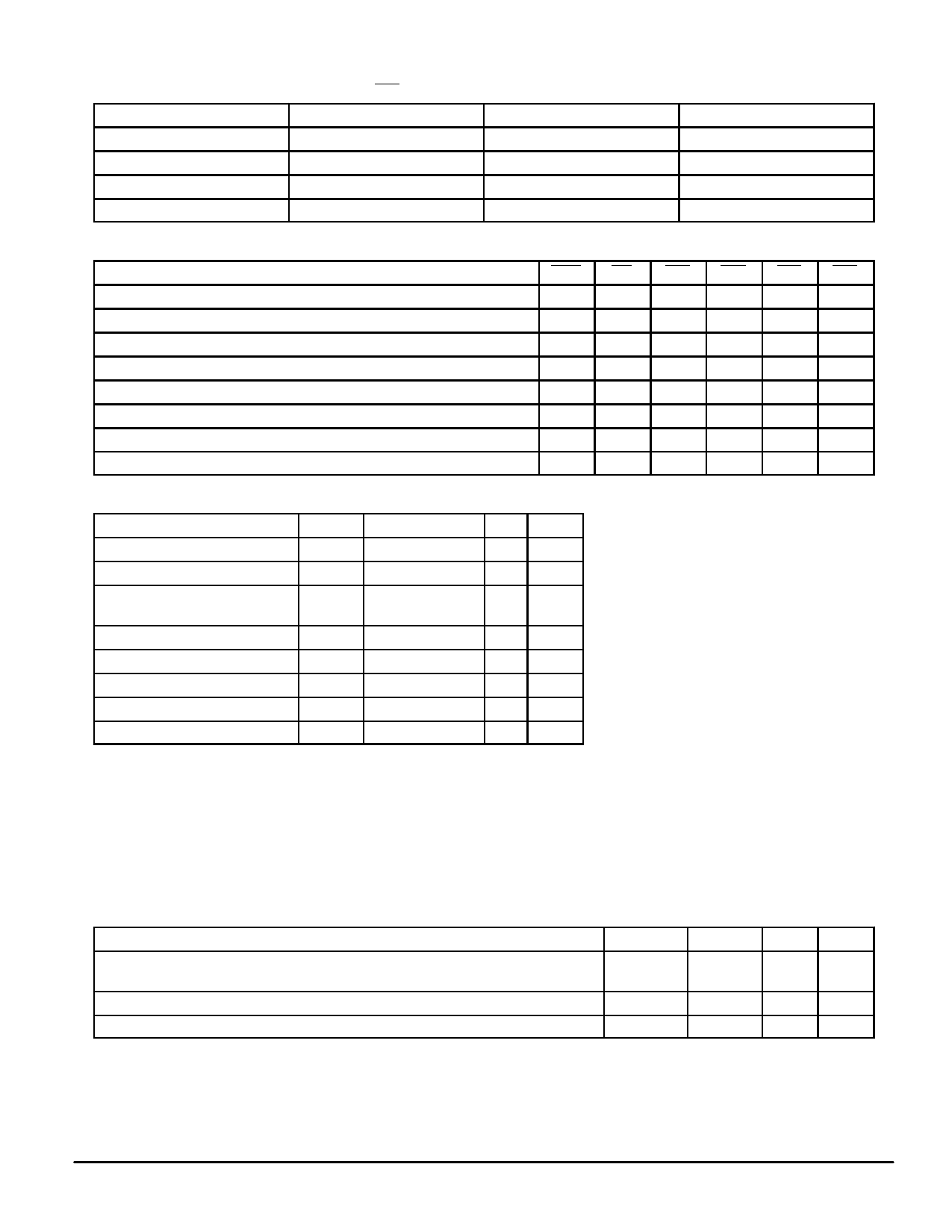
INTERLEAVED BURST ADDRESS TABLE (LBO = VDD)
1st Address (External)
2nd Address (Internal)
X . . . X00
X . . . X01
X . . . X01
X . . . X00
X . . . X10
X . . . X11
X . . . X11
X . . . X10
3rd Address (Internal)
X . . . X10
X . . . X11
X . . . X00
X . . . X01
4th Address (Internal)
X . . . X11
X . . . X10
X . . . X01
X . . . X00
WRITE TRUTH TABLE
Read
Read
Write Byte a
Write Byte b
Write Byte c
Write Byte d
Write All Bytes
Write All Bytes
Cycle Type
SGW SW
H
H
H
L
H
L
H
L
H
L
H
L
H
L
L
X
SBa SBb SBc SBd
X
X
X
X
H
H
H
H
L
H
H
H
H
L
H
H
H
H
L
H
H
H
H
L
L
L
L
L
X
X
X
X
ABSOLUTE MAXIMUM RATINGS (See Note 1)
Rating
Symbol
Value
Unit Notes
Power Supply Voltage
I/O Supply Voltage
VDD
– 0.5 to + 4.6
V
VDDQ VSS – 0.5 to VDD V
2
Input Voltage Relative to VSS for Vin, Vout – 0.5 to VDD + 0.5 V
2
Any Pin Except VDD
Input Voltage (Three–State I/O)
VIT – 0.5 to VDDQ + 0.5 V
2
Output Current (per I/O)
Iout
± 20
mA
Package Power Dissipation
PD
1.2
W
3
Temperature Under Bias
Tbias
– 10 to + 85
°C
Storage Temperature
Tstg
– 55 to + 125
°C
NOTES:
1. Permanent device damage may occur if ABSOLUTE MAXIMUM RATINGS are
exceeded. Functional operation should be restricted to RECOMMENDED OPER-
ATING CONDITIONS. Exposure to higher than recommended voltages for extended
periods of time could affect device reliability.
2. This is a steady–state DC parameter that is in effect after the power supply has
achieved its nominal operating level. Power sequencing is not necessary.
3. Power dissipation capability is dependent upon package characteristics and use
environment. See Package Thermal Characteristics.
This device contains circuitry to protect the
inputs against damage due to high static volt-
ages or electric fields; however, it is advised
that normal precautions be taken to avoid
application of any voltage higher than maxi-
mum rated voltages to this high–impedance
circuit.
PACKAGE THERMAL CHARACTERISTICS
Rating
Symbol
Max
Unit Notes
Junction to Ambient (@ 200 lfm)
Single–Layer Board
Four–Layer Board
RθJA
40
°C/W 1, 2
25
Junction to Board (Bottom)
RθJB
17
°C/W
3
Junction to Case (Top)
RθJC
9
°C/W
4
NOTES:
1. Junction temperature is a function of on–chip power dissipation, package thermal resistance, mounting site (board) temperature, ambient
temperature, air flow, board population, and board thermal resistance.
2. Per SEMI G38–87.
3. Indicates the average thermal resistance between the die and the printed circuit board.
4. Indicates the average thermal resistance between the die and the case top surface via the cold plate method (MIL SPEC–883
Method 1012.1).
MCM63P733A
6
MOTOROLA FAST SRAM
Share Link: 