AD5340BRU Просмотр технического описания (PDF) - Analog Devices
Номер в каталоге
Компоненты Описание
производитель
AD5340BRU
Analog Devices

AD5340BRU Datasheet PDF : 28 Pages
| |||
AD5330/AD5331/AD5340/AD5341
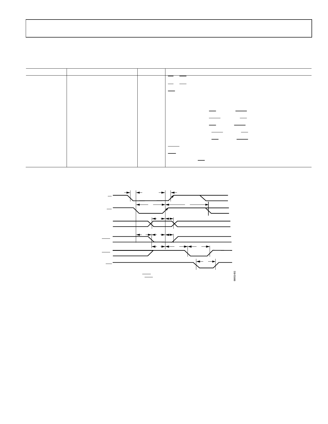
TIMING CHARACTERISTICS1, 2, 3
VDD = 2.5 V to 5.5 V, all specifications TMIN to TMAX, unless otherwise noted.
Table 3.
Parameter
t1
t2
t3
t4
t5
t6
t7
t8
t9
t10
t11
t12
t13
Limit at TMIN, TMAX
0
0
20
5
4.5
5
5
4.5
5
4.5
20
20
50
Unit
ns min
ns min
ns min
ns min
ns min
ns min
ns min
ns min
ns min
ns min
ns min
ns min
ns min
Condition/Comments
CS to WR setup time.
CS to WR hold time.
WR pulse width.
Data, GAIN, BUF, HBEN setup time.
Data, GAIN, BUF, HBEN hold time.
Synchronous mode; WR falling to LDAC falling.
Synchronous mode; LDAC falling to WR rising.
Synchronous mode; WR rising to LDAC rising.
Asynchronous mode; LDAC rising to WR rising.
Asynchronous mode; WR rising to LDAC falling.
LDAC pulse width.
CLR pulse width.
Time between WR cycles.
1 Guaranteed by design and characterization, not production tested.
2 All input signals are specified with tR = tF = 5 ns (10% to 90% of VDD) and timed from a voltage level of (VIL + VIH)/2.
3 See Figure 2.
CS
WR
DATA,
GAIN,
BUF,
HBEN
LDAC1
LDAC2
t1
t2
t3
t13
t4
t5
t6
t7
t8
t9
t10
t11
t12
CLR
NOTES:
1SYNCHRONOUS LDAC UPDATE MODE
2ASYNCHRONOUS LDAC UPDATE MODE
Figure 2. Parallel Interface Timing Diagram
Rev. A | Page 5 of 28
Share Link: